JTI Chip Antenna Mounting and Tuning Techniques
LTCC Chip Antennas –How to maximize performance
Outline
- Chip Antenna Characteristics
- Antenna Selection Considerations
- Circuit Design Constraints
- Layout Tips
Motivation
Chip Antenna an efficient means of “connectivity” to modern portable compact electronic devices.
Miniature portable devices requires small antennas.
Can be internalized – i.e. “Concealed” within device.
Pros & Cons
Pros:
Chip antennas are small, cheap and performs well.
Bulky external “whip” type antennas are thing of the past.
Cons:
Must be accounted for during initial circuit design stage.
Interference, proximity de-tuning & degradation concerns.
Ultimate Goal → To Maximize Performance
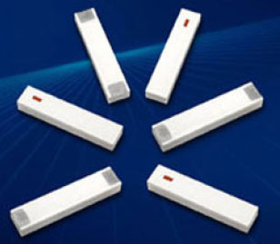
- Features Ag radiating element encapsulated in ceramic.
- A quarter-wave ( λ/4 ) monopole system.
- Works with GND plane to form dipole system.
- Certain “No-GND” metal-free space necessary.
- Small form factor, thin profile & light weight
- Omni-directional radiation.
- Linear Polarization.
- Mounting configuration flexibility.
- Frequency range supported: 0.08 GHz thru 10 GHz.
- WiFi, BT, WiMAX, UWB, GSM, CDMA, GPS etc.
- Suitable for Pick & Place.
- Size
- Frequency Band
- Bandwidth
- Polarization
- Peak Gain
- Average Gain
- Radiation Pattern requirements
- Successful Antenna design means harmonious interaction of the “seven” parameters (next page).
- Additional considerations for diversity systems – e.g. MIMO
- Overall performance is always system dependent.
- Size of the Circuit board.
- Layout of other board components.
- Complexity of circuit.
- Proper GND/No-GND dimensions and clearances.
- “Tuning” Matching Circuitry
- Shielding
- Suitable Enclosure (material)
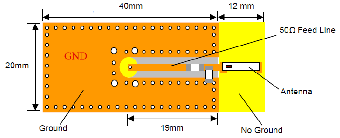
The ceramic chip antenna and top RF ground must be on the same plane. Substituting the top layer for an inner layer as a ground plane requirement will not work
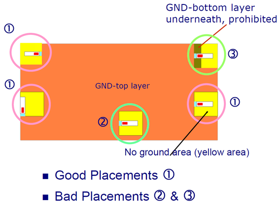
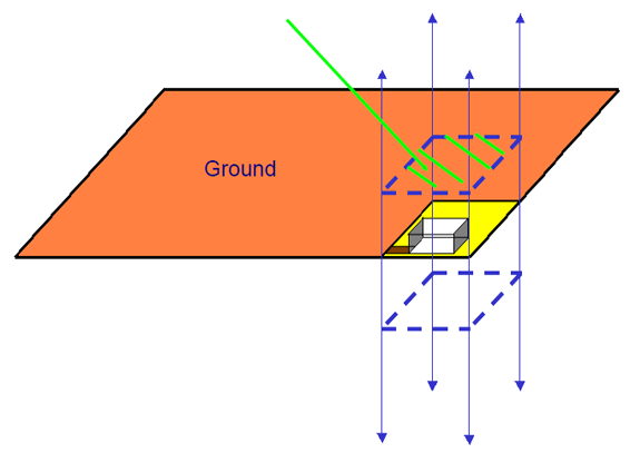
Don’t put any metal objects or batteries (if applicable) above or below the yellow region.
Keep away any other metals from clearance area.
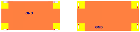
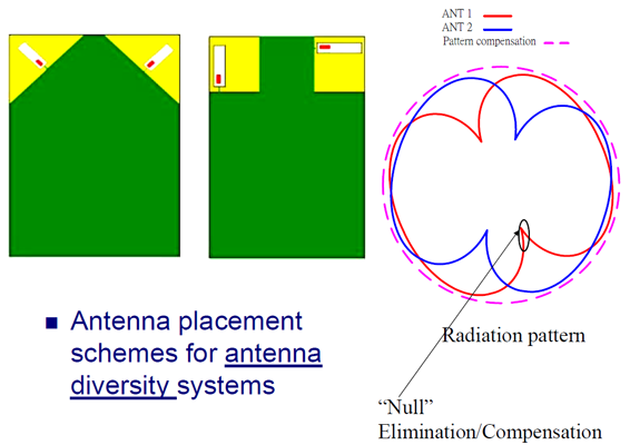
Further examples of good antenna placement schemes
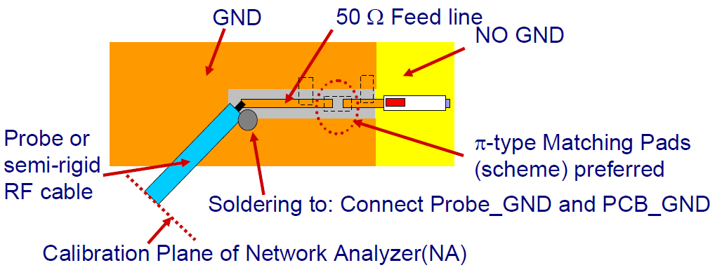
- One-port (S11) calibration for N.A. (Network Analyzer) Open-Short-Load for desired operating bandwidth
- Mount probe (semi-rigid RF cable for our example) onto PCB and connect to N.A.
- Measure S11 of test board without antenna or any matching components and save as: →S11_open →save trace to memory of N.A.
- Measure S11 of test board with antenna and series 0Ω resistor mounted and save as: →S11_antenna
- Set N.A. to data/memory mode (S11_antenna/S11_open) and display/save as: →S11_match
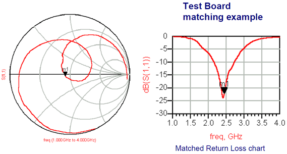
- Match the trace of S11_match to 50Ω (center of Smith chart at the desired frequency)
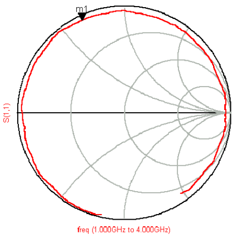
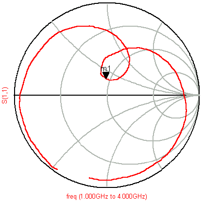
(not-normalized)
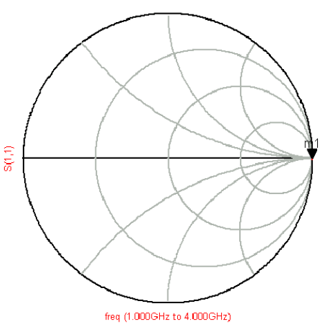
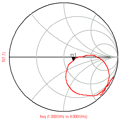
(normalized)
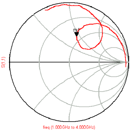
(normalized)
| Part Number | 2450AT45A100 |
|---|---|
| Frequency Range | 2400 - 2500 Mhz |
| Peak Gain | 3.0 dBi typ. (XZ-V) |
| Average Gain | 1.0 dBi typ. (XZ-V) |
| Return Loss | 9.5 dB min. |
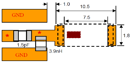
* matching circuit and component values will depend on PCB layout, thickness, material, etc.
JTI P/N for Matching Circuit: Cap (1.5pF): 500R07S1R5BV4T Inductor (3.9nH): L-07C3N9SV6T