Soldering Profiles and Guidelines for SMT Ceramic Components
General
Ceramic chip capacitors exhibit excellent reliability characteristic sproviding that proper circuit design techniques and controlled assembly processes are utilized. Due to ceramic capacitor’s crystalline micro-structure these components are susceptible when exposed to excessive thermal or mechnical shock during circuit processing. It should be noted that micro-cracks in ceramic can be difficult to detect with normal post assembly visual and electrical testing and can pose a significant threat to reliable field operation. For this reason it is reccommened that the assembly qualification process employ suitable testingto expose the presence of micro-cracking conditions.
Ceramic components’ leads composition and soldering compatibility
High Frequency Ceramic Capacitors & Inductors – Offered with standard tin plated nickel-barrier terminations compatible with solder flow and reflow process.
LASERtrim® Capacitors - Offered with gold flashed nickel- barrier terminations only. Due to the unique internal construction of the LASERtrim® it is recommeded that a convervative reflow temperature profile be used (Fig.4). Wave soldering is discouraged.
Soldering Iron
Ceramic capacitor attachment with a soldering iron is discouraged due to the inherent limitations on precisely controlling soldering temperature, heat transfer rate, and time. In the event that a soldering iron must be employed the following precautions are recommended.
- Preheat circuit and ceramic component to 150°C
- Never contact the ceramic surface with the iron tip
- 30 watt iron output (max)
- 280°C tip temperature (max)
- 3.0mm tip diameter (max)
- Limit soldering time to 5 sec.
Solder Pre-Heat Cycle
Proper preheating is essential to prevent thermal shock cracking of the capacitor. The circuit assembly should be preheated as shown in the recommended profiles at a rate of 1.0 to 2.0°C per second to within 65 to 100°C of the maximum soldering temperature.
SMT Soldering Temperatures
Solders typically utilized in SMT have melting points between 179°C and 188°C. Activation of rosin fluxes occurs at about 200°C. Based on these facts a minimum peak reflow temperature of 205°C to 210°C should be established. A maximum peak reflow temperature of 225°C should be adequate in most circumstances. Many reflow process profiles have peaks ranging from 240°C to 260°C and while ceramic capcitors and inductors can withstand soldering temperatures in this range for short durations they should be minimized or avoided whenver possible. Use of PCB mounted multiple thermocouple M.O.L.E. profiling is advised for accurate characterization of circuit heat absorption and maximum temperature conditions.
Reflow Solder
The general term "reflow" refers to several methods used in heating the circuit so that solder paste reflows, or "wetting" of the ceramic capacitor and PCB contacts occurs. These methods include infrared, convection and radiant heating. The size of the solder fillet may be controlled by varying the amount of solder paste that is screened onto the circuit. Recommended temperature limits and times for solder reflow are shown in Figure 1 for Ceramic Capacitors, Inductors and for LASERtrim® in Figure 4.
Vapor Phase
A typical vapor phase soldering process consists of several temperature zones created by saturated vapor from a boiling liquid. As the circuit passes through the zone the vapor condenses on the solder paste, pad, and termination resulting in heat transfer and reflow of the solder paste. Vapor phase reflows produces consistent circuit heating with reflow occurring at a relatively lower temperature that is determined by the known boiling point of the liquid used, typically 215°C. Recommended temperature limits for vapor phase reflow are shown in Figure 2.
Solder Wave
Wave soldering is perhaps the most rigorous of surface mount soldering processes due to the steep rise in temperature seen by circuit as it is immersed in the molten solder wave, typically at 240°C. Recommended temperature limits for wave soldering are shown in Fig 3.
Cool Down Cycle
After the solder reflows properly the assembly should be allowed to cool gradually at room ambient conditions.
Attempts to speed this cooling process or immediate exposure of the circuit to cold cleaning solutions may result in thermal shock cracking of the ceramic capacitor.
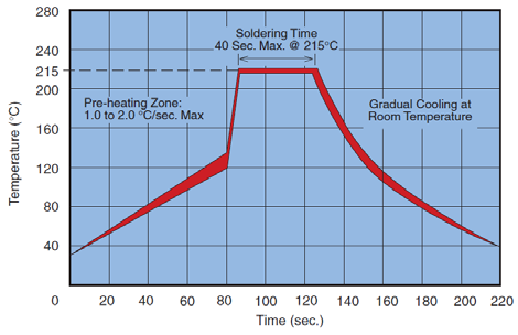
Figure 2: Vapor Phase Profile for MLCCs
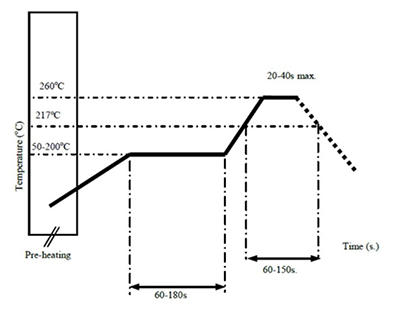
Figure 1: Solder Reflow Profile for Ceramic Capacitors and Inductors (JEDEC J-STD-020C compatible)
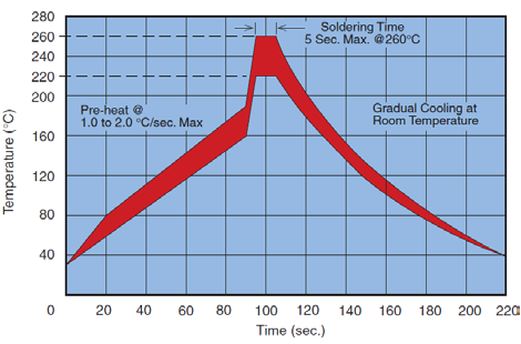
Figure 3: Wave Solder Profile for MLCCs
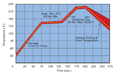
Figure 4: Solder Reflow Profile for LASERtrim®
Solder Fillets
To avoid detrimental effects of thermal and mechanical stress it is essential that the solder fillet be limited to 2/3rds of the overall height of the MLC termination as illustrated in the figure below. The solder fillet can be controlled by solder paste deposition and pad design in reflow and vapor phase processes and by pad design and use of hot air knives in the wave process. As shown in Figure 5.
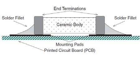
Figure 5
Tomb-Stoning/Chip Movement
Tomb-stoning or draw birding is illustrated in the figure below. Tomb-stoning or other undesirable chip movements may result if unequal surface tension forces exist as the molten solder wets the MLC terminations and mounting pads. This tendency can be minimized by insuring that all factors at both solder joints are equal, namely; pad size, solder mass, termination size, component position and heating. Tomb-stoning is easily avoided through proper design material selection and proofing of the process. As shown in figure 6.
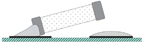
Figure 6