Understanding Chip Capacitors
BASIC CAPACITOR INFORMATION
Capacitors are electrical energy storage devices used in the electronics circuits for varied applications notably as elements of resonant circuits, in coupling and by-pass application, blockage of DC current, as high frequency impedance matching and timing elements, as filters in delay-line components, and in voltage transient suppression.
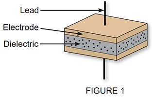
The capability of storing electrical charge was first discovered in Holland by Pieter van Musschenbroek in the 18th century. This first capacitor consisted of a water-filled glass jar charged with static electricity. As is well known, the famous British scientist, Michael Faraday, determined later in the 18th Century the nature of electricity and capacitance. The charge stored in any device is proportional to the voltage applied (Q=CV). The capacitance C, expressed in Farads, is in turn dependent on the properties of the dielectric material, and the geometry of the device, namely, the area of the electrodes and the thickness of the dielectric between electrodes.
The capacitance for a single plate device can be determined as follows:
Where k = relative dielectric constant
of the insulator between the electrodes
A = Area of overlap of the electrodes
t = Thickness of Dielectric
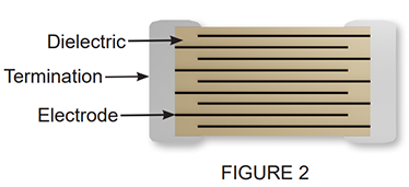
Monolithic multilayer construction maximizes the geometric factor by incorporating a large electrode area into a small volumetric package. This is achieved by stacking many layers which are laminated to produce the device shown in Figure 2.
This construction using high k ceramic dielectrics with high dielectric strength, permits the manufacture of chip capacitors with high layer counts. As a result, these capacitors exhibit very high volume efficiency
When calculating capacitance:
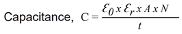
Where:
k = Dielectric Constant of Material
A = Area of Overlapping conductive plates
t = Thickness of Dielectrics between the plates
N = (number of overlapping electrodes - 1)
The complex permitivity Ɛ is calculated as follows:
CAPACITOR ELECTRICAL PROPERTIES
In order to understand the dielectric ceramic materials, some prerequisite knowledge of the electrical properties of dielectrics are required.
In addition to the capacitance, other highly significant properties must be considered, especially as capacitors are used in AC applications.
Dielectric Constant (k):
The dielectric constant achieved in any insulator material occurs due to interactions between an applied electric field and localized charge centers within the dielectric. Charges are not transferred, but displaced by the field, ie: positive charges shift towards the negative electrode, and negative charges become displaced towards the positive electrode. In ceramic dielectrics with high dielectric constant, easily polarizable charges shift, creating a polarization effect which opposes the electric field applied, thus drawing more charge onto the electrodes.
The polarization effect arises from four (4) mechanisms:
1) Electronic displacement: The atom’s electron cloud is displaced from the center of symmetry of the atom; positive nucleus and negative electron cloud center no longer coincide generating a dipole effect. This effect is common of all materials.
2) Ionic displacement: The electric field induces displacement of the positive and negative ions, creating a dipole moment. In BaTi03 (perovskite) type ferroelectric* structures, this displacement is relatively large, and is the main contributing mechanism to the dielectric constant.
3) Permanent dipole orientation: This mechanism is predominant in polymers, and not a major contributor to polarization in ceramic as the rigid crystal structure precludes motion of fixed dipoles.
4) Space charge polarization: This process is dependent on the presence of mobile charges in the structure which migrate partway toward the electrodes, creating a polarizing effect.
The net polarization contribution to the dielectric constant is the summation of the above processes. These processes, in turn, are greatly affected by temperature, DC bias, frequency, and AC voltage.
Capacitors, notably those made with ferroelectric dielectrics, therefore experience a variance in dielectric constant, and hence capacitance, under differing environments and test conditions. The effects of these variables are explained and related to specific dielectrics in following sections of the text.
* Ferroelectric materials display a hysteresis effect of polarization under an alternated applied field, analogous to a ferromagnetic hysteresis loop (induction vs magnetic field), hence the term “ferroelectricity”.
Dissipation Factor / Power Factor
When voltage is applied to a capacitor, a charging current will flow; this current will delay the buildup of the full applied voltage generating a time displacement of the alternating voltage behind the current.
In a “no-loss” perfect capacitor, the phase difference between voltage and current would be exactly 90°. In a real dielectric, however, this ideal phase angle is inhibited for two (2) reasons:
a) No dielectric is a 100% perfect insulator, hence, a small degree of leakage occurs.
b) The polarization mechanisms of the ceramic, which must take place in order to store electrical charge, are not 100% efficient; the capacitor does not discharge 100% of the energy absorbed in the charging cycle. Furthermore, these mechanisms, notably space charge, dipolar, ionic, and electronic polarization are highly dependent on frequency and dielectric composition. The losses incurred due to a lag of the polarization with frequency are known as “relaxation losses” and manifest themselves as heat and a deviance from the 90° lead in the current to voltage phase (Figure 3).
The dissipation factor (DF) is the tangent of the angle by which the current lags from the 90° vector to the voltage (Figure 3), and it is more often expressed as Percent Dissipation Factor (%DF), ie: DF of .001 is expressed as 0.1%. The Power factor is the cosine of the phase angle between the voltage and current vectors (Cosθ). For low-loss dielectrics, tan∂ and Cosθ are nearly equal, and often used interchangeable when expressing dielectric loss
I: Ideal Current Vector
It: True Current Vector
v: Voltage Vector
Current Voltage Phase
Quality Factor (Q)
In simple terms, the quality factor Q is the reciprocal of the loss factor.

A near-perfect capacitor, or a high Q capacitor, therefore, has a Q approaching infinity. The Q factor is dependent on the frequency, ie: the polarization mechanisms operating at any given frequency.
Temperature Coefficient (TC)
The temperature coefficient (TC) of a ceramic dielectric defines the deviance in capacitance which occurs over a given temperature range. Ceramic dielectrics, notably those consisting of BaTi03, experience variation in dielectric constant over temperature due to crystallographic inversions and thermal energy effects on the Ti atom mobility. Minor additions, which suppress or shift the temperature characteristic of BaTi03 are used to formulate dielectrics with discrete temperature characteristics.
The TC is expressed as percent capacitance change, or ppm/°C variance from the 25°C reference measurement. Typical TC curves are shown in the following Figures 4 and 5:
The temperature characteristic of the higher k (ferroelectric) dielectrics is most often expressed as % cap change vs temperature, as shown in Figure 4, for the X7R dielectric. The temperature characteristic of the linear dielectrics (NP0 and temperature compensating) is expressed in ppm/°C The TC in ppm/°C is calculated for any temperature range using the following expressions
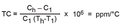
- Where: Th = Higher temperature
- T1 = Lower temperature (reference)
- Ch = Capacitance at Th
- C1 = Capacitance at T1
- Example:
- Capacitance @ -55°C = 7685 pF
- Capacitance @ 25°C = 7690 pF
- Capacitance @ 125°C = 7683 pF
TC for 25°C →125°C range
Th = 125°C Ch = 7683 pF
T1 = 25°C C1 = 7690 pF (reference)
- Example:
- Slope from RT (25°C) reference to 125° C is -9.1 ppm/°C
- Computation for the lower portion of the curve (-55°C →25°C)
Th = 25°C Ch = 7690
T1 = - 55°C C1 = 7685
Example:
Slope from -55°C reference to 25°C is + 8.1 ppm/°C
Dielectrics are formulated to meet TC requirements called for by the MIL and EIA specifications, or customer.
The temperature characteristics are used to classify dielectrics, as outlined in the section of the text under “General Classes of Dielectrics.”
DC Voltage Coefficient(VC)
Ceramic dielectrics based on ferroelectric formulations will experience a decrease in dielectric constant of capacitance with increased voltage (DC) bias. This variance occurs due to the restriction that voltage stress causes on the freedom of some of the polarization mechanisms. Increased DC bias (more volts/mil of dielectric) will inhibit portions of the polarization cycle which oppose the DC bias.
The voltage coefficient becomes more severe with higher k dielectrics, which have ferroelectric domain orientation (shifting of ionic dipoles), as the major polarizing mechanism. (Figure 6 shows ΔC vs VDC/mil bias for higher k dielectrics).
The voltage coefficient thus, is an important consideration in the design of chip capacitors. The dielectric thickness must be chosen such that the volts/mil at operating voltage does not create a capacitance loss which exceeds specifications.
Temperature Voltage Coefficient (TVC)
As many Class II capacitors must operate at rated voltage over a specified temperature range, it is necessary that the combined effect of temperature and voltage (TVC) be considered in the design and manufacture of capacitors. The TVC for any chip can be measured at rated voltage over the temperature range or estimated by combining the known TC and VC data for any given dielectric and volts/mil bias, as shown in Figure 6.
Class I capacitors (NP0) are stable over temperature and voltage, and do not exhibit the behavior below.
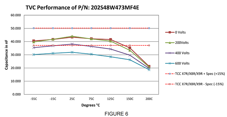
Figure 6 illustrates the change in capacitance due to temperature and voltage in one plot. In general, the capacitance drops as increasing voltage is applied to Class II capacitors. Temperature also affects the capacitance, which varies between the dielectrics.
When choosing capacitors, designers may wonder if there are really significant differences between an X7R capacitor with the same size and capacitance from different suppliers. There can be significant differences. Requesting a plot such as Figure 6, can help designers differentiate between the performance of different capacitors of similar nominal characteristics.
It is very important to ensure the capacitor chosen meets the electrical and environmental requirements for the intended application. Johanson is able to provide this information to customers upon request.
Insulation Resistance (IR)
The insulation resistance is a measure of the ability of the charged capacitor to withstand leakage of DC current. Variations in value of insulation resistance can occur due to:
a) Change in surface resistivity, due to moisture or other adsorbed contaminants.
b) Change in bulk dielectric resistivity, due to intrinsic (material) or extrinsic (chip structure) causes.
Intrinsic conductivity (ie: Reduction of the insulation resistance) in ceramic dielectrics arises due to ionic charge carriers which are mobile due to atomic lattice defects. These ions will move from one atomic interstitial site to another under the influence of an electric field, hence generating leakage of DC current. The mobility of the charge carriers increases with temperature; all dielectrics thus display a considerable drop in insulation resistance when measured at the higher (125°C) temperature limits of the MIL specifications.
In addition to the above process, titanate dielectrics are subject to variability in insulation resistance, due to sensitivity of their electrical properties to stoichiometry (ratio of oxygen to cations in the crystal lattice). Titanate dielectrics, in fact, can easily become semiconductors with minor changes in stoichiometry. Deviation from ideal valency, ie: the ratio of positive to negatively charged ions, will generate unbalanced charges that will transfer along a potential gradient. The formulation and processing of titanate dielectrics therefore requires extreme accuracy in order to maintain adequate insulation resistance.
In practice, it is found that the value of the insulation resistance is also strongly related to the chip design, number of dielectric layers, area of layers, thickness of dielectric, physical quality of structure, and test conditions. These are the extrinsic factors affecting I.R., and must be considered when evaluating chip capacitors.
Higher capacitance value chips are made with more, or thinner, dielectric layers, or larger electrode plates than units of lesser value, built with the same dielectric. The probability of the occurrence of the mechanisms which lower the resistance therefore increases with higher value capacitors.
The insulation resistance, calculated as the product of R X C, is a constant for any given dielectric, regardless of the capacitance value, as long as surface resistivity and extrinsic variables (chip structure) are constant. It is for this reason that insulation quality of higher value capacitors (>.01 µF) is reported as the product of the I.R. and capacitance; ohm-farads (ΩF), or Megaohm-Microfarads (MΩµF). MIL-PRF-55681 requires that the ΩF product exceed 1000 for values equal to or above .01 µF. For values below .01 µF, the ΩF product is not applicable, as very high resistances in the TΩ to ∞ region (which are difficult to measure accurately) are typical. The general requirement for capacitors <.01 µF is that the I.R. exceed 1000,000 MΩ (1 TΩ).
Table I lists the minimum I.R. required for the full series of RETMA values. RETMA values refer to a system of standardized numbernig of part values. It was developed in 1924 by a United States-based radio manufacturers trade group known as the "Associated Manufacturers."
TABLE I
Minimum I.R. Requirement vs Retma Value
At 25°C; 125°C is 10% 25°C Specification
| 1.0pF | 100GΩ |
| ↓ | ↓ |
| .010µF | 100GΩ |
| .012µF | 83.3GΩ |
| .015µF | 66.6GΩ |
| .018µF | 55.5GΩ |
| .022µF | 45.4GΩ |
| .027µF | 37.1GΩ |
| .033µF | 30.3GΩ |
| .039µF | 25.6GΩ |
| .047µF | 21.3GΩ |
| .056µF | 17.9GΩ |
| .068µF | 14.75GΩ |
| .082µF | 12.12GΩ |
| .100µF | 10.0GΩ |
| .120µF | 8.4GΩ |
| .150µF | 6.6GΩ |
| .180µF | 5.6GΩ |
| .220µF | 4.5GΩ |
| .270µF | 3.7GΩ |
| .330µF | 3.0GΩ |
| .390µF | 2.5GΩ |
| .470µF | 2.1GΩ |
| .560µF | 1.8GΩ |
| .820µF | 1.2GΩ |
| 1.000µF | 1.0GΩ |
For reference:
1 MΩ = 106Ω M = MEGA
1 GΩ = 109Ω G = GIGA
1 TΩ = 1012 Ω T = TERA
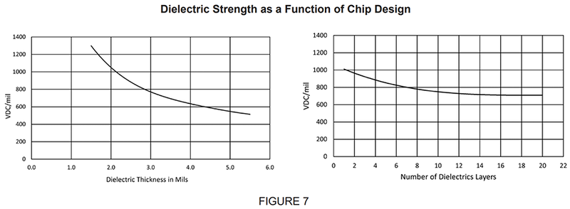
Dielectric Strength
The dielectric strength is defined as the voltage gradient which produces electrical breakdown of the capacitor. This voltage is a function of the material and thickness of the dielectric layer tested.
Analogous to the Insulation Resistance of ceramic capacitors, determinations of dielectric strength, or “flash” failure, must be related to the capacitor in question; dielectric breakdown is reported as volts/mil, or volts/cm of dielectric. Capacitors are designed with sufficient thickness of dielectric to provide a margin of safety, ie: volts/mil loading at flash voltage is well below the breakdown value for the dielectric. In addition to this consideration, the dielectric thickness selected must meet the voltage coefficient requirements discussed previously.
Dielectric failure can originate from several causes. Units tested at high voltages (>1000 VDC), must be immersed in dielectric fluid to prevent arcing over the external surfaces. This applies notably to small capacitors, where external surface failures become more likely at higher voltages. In application, high voltage capacitors must be potted in an insulating compound to preclude external dielectric failure. Breakdown of the dielectric layer in a ceramic chip is attributed to a combination of two (2) processes, which are generated at high field loading:
Thermal Failure: High Voltage stress activates the dielectric loss processes, generating heat, which, in turn, lowers the resistivity of the material to the point where, with sufficient time duration, current is channeled along the weakest path between any two plates of the capacitor, resulting in puncture.
Electronic or Intrinsic Failure: The voltage stress energizes electrons at localized points in the structure and are accelerated along the voltage gradient, colliding with and energizing other electrons, thus generating an avalanche effect which ultimately causes breakdown.
Unlike the thermal breakdown process, electronic dielectric strength increases with temperature, as increased atomic lattice vibrations inhibit electron flow.
The probability of occurrence of weaker dielectric zones increases with thickness, area, and number of plates in a capacitor. As is expected, higher (volts/mil) dielectric strengths are obtained with the smaller capacitors, constructed with fewer and thinner dielectric layers (Figure 7). In practice, the design of capacitors is regulated by the size, capacitance, dielectric, and voltage called for by the customer; dielectric thickness and number of layers used to build any capacitor are selected to meet the customer requirements with a margin of safety, which brings the voltage stress well below the actual breakdown threshold of the ceramic.
Ageing
Ferroelectric dielectrics exhibit a time dependence of dielectric constant and dielectric loss known as “Ageing.” It is theorized that this behavior is due to strain energy of the ferroelectric domains striving form orientation relative to one another after their formation. Domains appear in ferroelectrics of the BaTi03 (perovskite) structure after cooling past the Curie Temperature, the temperature where the structure goes from a cubic (paraelectric) to a tetragonal (ferroelectric) crystal habit.
The relaxation or continued orientation of the ferroelectric domains generates a logarithmic decay of the dielectric constant (k) with time, expressed as:
k = Ko-M log t
Where k = dielectric constant at t hours:
ko = initial dielectric constant (at time of first measurement)
M = slope or rate of decay
As seen from the above expression, the ageing curve for any dielectric is a straight line function, if plotted on semi-log paper, and will be largely dependent on the initial dielectric constant ko (ie: rate of ageing increases as ko increases), as shown in Figure 8.
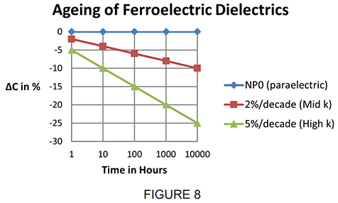
The ageing rate of capacitors is expressed in terms of “decade hours”. In the example in Figure 8, K2000 dielectric ages 2% / decade hour, ie: capacitors will lose:
a) 2% between 0.1 and 1 hour after cooling through the Curie Point
b) An additional 2% between 1 and 10 hours after cooling through the Curie Point
c) An additional 2% between the following 10th and 100th hours, etc.
Capacitors displaying the ageing behavior consequently must be sorted for capacitance tolerance at discrete time periods after the final transition through the Curie point.
The complex microstructure of the polycrystalline ceramic structure also affects the time dependence of k. The domain strain energy is dependent on the volume and size of pores, impurities present, the grain size, and the nature of the grain boundaries; in short, ageing is a variable of composition processing, and firing of capacitors.
The ageing behavior of ferroelectrics is reversible, as heating the dielectric beyond the Curie point reverts the structure to the paraelectric state. Subsequent cooling therefore reinstates the strain energy of the domains, and the ageing process begins anew. The temperatures used in capacitor attachment processes in many cases exceed the Curie point of the ferroelectric (high k) dielectrics. Users of high k chips will therefore find a temporary increase in capacitance of their units when attached to PCB circuit board with soldering, solder-reflow, or thermos-compression attachment methods.
The ageing of high k dielectrics can be “stabilized,” or minimized to some degree by heating of units to a temperature near the Curie point, under the influence of a DC bias. This voltage conditioning effect will accelerate the ageing process by one or more decades, depending on the dielectric and DC bias in question.
SRF/PRF of RF Capacitors
Capacitors exhibit both series and parallel resonant frequencies. There is a frequency for a capacitor with a given physical size/construction and a given capacitance value at which the component looks like an inductive impedance. Indeed, above this frequency one can have essentially a “DC blocking inductor”. This frequency is called the Series Resonant Frequency (SRF). The magnitude of the transmission impedance the capacitor presents will be extremely low from the bottom frequency determined by the capacitance value, up through the SRF until one approaches the first Parallel Resonant Frequency (PRF). The first PRF is frequently called simply the PRF, although in reality there is a second PRF, third PRF, and so on. A rough rule of thumb puts the PRF at twice the frequency as the SRF, although some designs vary significantly. The magnitude of the transmission impedance dip differs significantly at each PRF frequency, and with the various values of capacitors.
Exactly at the SRF, one will have the lowest possible impedance, and therefore, a capacitor is commonly used for narrow band RF bypass applications by choosing a capacitor whose SRF is at the required bypass frequency. In other words, at the SRF, the capacitive impedance of the device equals the parasitic inductive impedance of the device. The user is only left with the ESR (no reactive component) at that frequency.
For applications where low impedance is desired, but it is unimportant if the capacitor looks either capacitive or inductive, a capacitor could be used up to a frequency close to the PRF. Above the SRF, the user essentially has a “DC blocking inductor”. At the PRF, the transmission impedance goes relatively high, and the capacitor is virtually useless around this frequency. There is an industry “trick” to effectively extend the usable frequency range in this application. That is to mount the capacitor in a vertical position so that the capacitor terminations both still meet the pads where it’s mounted, and so the width of the capacitor is now effectively the height. Doing this will eliminate all odd-order PRFs including the first PRF.
EFFECTS OF PARALLEL (HORIZONTAL) VS VERTICAL MOUNTING (ORIENTATION)
The orientation of the capacitor when mounted on the circuit board can affect the SRF. Figure 9 illustrates parallel (horizontal) mounting where the electrodes are parallel to the substrate surface and the electrical effect for a given capacitor value. Figure 10 illustrates vertical mounting where the electrodes are perpendicular to the substrate surface and the electrical effect for the same given capacitor value.
The PRF effects are due to very complex mechanisms related to the different phase paths to the various electrodes of the multi-layer capacitor. At Johanson, we typically measure the S-parameters in a normal orientation (per Figure 9) showing the first PRF, allowing the user to optionally mount it vertically which will eliminate the first PRF.
For matching applications, it is extremely important as to whether the component looks like a capacitor or an inductor. In this application, a designer will almost always want to be well below the SRF of the capacitor. It can be said that, for example, a 10pF capacitor could look like a 1000pF capacitor as the SRF is approached.
See Figure 11 above for Johanson SPICE equivalent circuit for a capacitor. The values shown are for a typical 10 pF capacitor at 900 MHz. This model tends to give a better SPICE simulation than the more common model where Cs represents the essential C at low frequencies, and Cp (if a Cp is even in the model) represents a fraction of Cs, even though this more common model is more conceptually easy to understand. Keep in mind that even our improvedmodel’s accuracy is not ideal at RF frequencies because the elements of this model themselves have a given ependence on frequency. In our model, at low frequencies, the parallel equivalent of Cs and Cp give the essential capacitance. Cs and Ls in our model are what give us the SRF effect. The network of Ls in series with Cs; which is in parallel with Cp is what gives us the first PRF effect. Note also that our model (and the common model) has no provision for simulating a second PRF. Rp is in our model for a more accurate simulation of what the capacitor looks like at RF frequencies, so don’t put an ohmmeter across a capacitor looking for Rp at DC where the Insulation Resistance will be typically greater than 10,000 Ohms.
Johanson offers, JTISoft, an electrical characteristics modeling tool that displays data and charts for Johanson High-Q capacitors. This tool is available at: https://jtisoft.johansontechnology.com/
Q and ESR
One of the most important parameters in evaluating a high frequency chip capacitor is the Q factor, or the related Equivalent Series Resistance (ESR).
In theory, a “perfect” capacitor would exhibit an ESR of 0 (zero) ohms and would be purely reactive with no real (resistive) component. The current going through the capacitor would lead the voltage across the capacitor by exactly 90 degrees at all frequencies.
In real world usage, no capacitor is perfect, and will always exhibit some finite amount of ESR. The ESR varies with frequency for a given capacitor, and is “equivalent” because its source is from the characteristics of the conducting electrode structures and in the insulating dielectric structure. For the purpose of modeling, the ESR is represented as a single series parasitic element. In past decades, all capacitor parameters were measured at a standard of 1 MHz, but in today’s high frequency world, this is far from sufficient. Typical values for a good high frequency capacitor of a given value could run in the order of about 0.05 ohms at 200 MHz, 0.11 ohms at 900 MHz, and 0.14 ohms at 2000 MHz.
The quality factor Q, is a dimensionless number that is equal to the capacitor’s reactance divided by the capacitor’s parasitic resistance (ESR). The value of Q changes greatly with frequency as both reactance and resistance change with frequency. The reactance of a capacitor changes tremendously with frequency or with the capacitance value, and therefore the Q value could vary by a great amount. See Equations 1 and 2.
Ripple Current
Ripple current is the AC current that the flows in and out of the capacitor as it is being used in a circuit. This causes heat to be generated within the capacitor, which then causes the temperature of the capacitor to rise. This internal heating can degrade the performance of the capacitor dielectrics, which have higher k values such as X5R and X7R as opposed to NP0 or High-Q NP0. Johanson makes a significant effort to publish measured ESR data using today’s industry accepted method such as the RS-483. Higher ESR components can be measured using capacitor meters.
The PCB pad is another factor which determines how much heat is exchanged from the capacitor onto the trace. Johanson’s recommended landings are optimized for RF/Signal performance. The IPC standard https://www.ipc.org/ipc-standards specifies for larger pads, but only the designer will know where the compromise is for the application.
To determine the rate of heat generation in a capacitor, this formula can be used:
P = I^2 * R → Pdis = (Irms)^2 x ESR
Where:
ESR = equivalent series resistance
Irms = rms value of the ripple current
Voltage Breakdown
The dielectric material of a capacitor has a dielectric strength which determines the voltage breakdown. Voltage breakdown occurs when the voltage applied to a capacitor exceeds the rated voltage. This can melt the dielectric which will destroy the capacitor. In other words, voltage breakdown limits the maximum energy that can be stored safely in a capacitor.
Factors that can affect voltage breakdown are humidity, pressure, temperature, as well as the geometry of the capacitor conductive parts.
dV/dt
dV/dt is the rate at which the voltage changes over time. Capacitors tend to resist changes in voltage drop. When voltage across a capacitor is increased or decreased, the capacitor resists the change by drawing current to the source of the voltage change, in opposition to the change.
Q = CV
Where:
Q = charge
V = voltage difference between two plates
C = capacitance
- Take derivative with respect to t on both sides
- dQ/dt = C dV/dt = i
- i=CdV/dt (remember I-V diagram)
- current = constant X time derivative of voltage
- Ohm’s law tells us about the relationship between V and I for a resistor. This equation describes the relationship between i and V for a capacitor.
GENERAL CLASSES OF DIELECTRICS IN CAPACITORS
Dielectrics are classified into types based on temperature characteristics and are identified by MIL or EIA designations.
Class I Dielectrics
Class I Dielectrics have linear temperature coefficient, and are defined in EIA and MIL specifications. These are lower k dielectrics (<150), consisting primarily of TiO2 with additions of Ba0, La203, or Nd205. The extended higher k dielectrics are near linear with (negative) temperature coefficients exceeding N 1500. These compositions have a dielectric constant ranging from 140 to approximately 500, and are based on CaTi03, SrTi03, MgTi03, and BaTi03: CaZrO3 mixtures.
Class I capacitors are used in circuits which require stability as low-loss (high Q) of dielectric characteristics over the full temperature range, with the following basic requirements:
a) Negligible time dependence of capacitance and dissipation factor (no ageing)
b) Predictable linear temperature coefficient
c) Low loss DF< 0.1% @ 1 MHz, TC series, <0.2% @ 1 MHz extended range series
d) Negligible dependence of capacitance and dissipation factor on voltage and frequency
Examples of Class I dielectric EIA designations and typical temperature characteristics are shown in Table II:
TABLE II
CLASS I - CERAMIC CAPACITORS
Letter codes for temperature coefficients α referring to EIA-RS-198
| Temperature Coefficient α 10-6°K Letter Code |
Multiplier of the Temperature Coefficient Number Code |
Tolerance of the Temperature Coefficient Letter Code |
|---|---|---|
| C: 0.0 | 0: -1 | G: ±30 |
| B: 0.3 | 1: -10 | H: ±60 |
| L: 0.8 | 2: -100 | J: ±120 |
| A: 0.9 | 3: -1000 | K: ±250 |
| M: 1.0 | 4: +1 | L: ±500 |
| P: 1.5 | 6: +10 | M: ±1000 |
| R: 2.2 | 7: +100 | N: ±2500 |
| S: 3.3 | 8: +1000 | |
| T: 4.7 | 8: +1000 | |
| V: 5.6 | ||
| U: 7.5 |
For example: C0G is TC 0.0, -1, ±30ppm/K
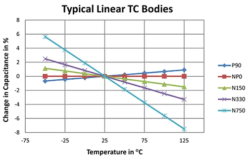
FIGURE 12
EXAMPLES:
COG = NP0 ± 30 ppm / °C
M7G = P100 ± 30 ppm / °C
P3K = N1500 ± 250 ppm / °C
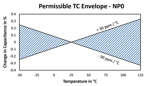
FIGURE 13
The TC requirements have permissible tolerances, which, if expressed graphically show an “envelope” within which the temperature characteristic may fall, as shown for NP0 (C0G) dielectric.
Class II Dielectrics
The higher k dielectrics (k>500) require the use of ferroelectric formulations based on BaTi03, which exhibit non-linear characteristics and less stable overall properties, namely:
a) Non-linear TC
b) Time dependence of capacitance and dissipation factor
c) Voltage (AC & DC) dependence of capacitance and dissipation factor
d) Frequency dependence of capacitance and dissipation factor
This class of dielectric materials is further subdivided into two (2) groups:
a) “MID k” stable Class II dielectrics, which meet MIL X7R, BX, BR, BQ, BZ and EIA X7R requirements.
b) High k (k>4000) formulations which meet EIA RS198B high k dielectric requirements.
These components are less stable, for the high dielectric constant is achieved by formulation of the
ceramic with the Curie point (peak k) at, or near, room temperature.
Class II dielectrics find application as by-pass and coupling components in circuitry where the stability of electrical properties can be sacrificed for the higher volume efficiency offered by the mid and high k dielectrics.
EIA designations for Class II dielectrics are shown in Table III:
TABLE III
CLASS II - CERAMIC CAPACITORS
Code system regarding to EIA RS-198 for some temperature ranges and inherent change of capacitance
| Letter Code Low Temperature |
Number Code Upper Temperature |
Letter Code Change of Capacitance Over the Temperature Range |
| X = -55°C (-67°F) | 4 = +65°C (+149°F) | P = ±10% |
| Y = -30°C (-22°F) | 5 = +85°C (+185°F) | R = ±15% |
| Z = +10°C (+50°F) | 6 = +105°C (+221°F) | L = ±15%, +15/-40% above 125°C |
| 7 = +125°C (+257°F) | S = ±22% | |
| 8 = +150°C (302°F) | T = +22/-33% | |
| 9 = +200°C (392°F) | U = +22/-56% | |
| V = +22/-82% | ||
| For example: X7R is -55/+125°C, ΔC/C0, ±15% C0 = C @ 25°C |
The dielectric types most commonly used are NP0 (Class 1), BX, X7R (Class II -mid k).
Table IV compares the characteristics of these dielectrics.
TABLE IV
| NP0 | DIELECTRIC COMPARISONBX, BR, BQ, BZ |
X7R | |
|---|---|---|---|
| Specification Sources Chip Requirements |
Military EIA | Miltary | EIA |
| Capacitance & Tolerance | As specified | As specified | As specified |
| D.F. (Max) | 0.1% / 0.2% | 2.5% | 2.5% |
| Temperature Performance Range | -55 thru 125°C | -55 thru 125°C | -55 thru 125°C |
| ΔC Tolerance | ±30ppm/°C | ±15% | +22% -56% |
| ΔC (with rated bias) | ±30ppm/°C | +15 -25% | Not required |
| IR @ 25°C | 1000ΩF | 1000ΩF | 1000ΩF |
| IR@upper temp limit | 100ΩF | 100ΩF | Not required |
| Life Test (max rated temp) | 100 hr, 2X | 1000 hr, 2X | 250 hr, 2X |
| Flash Test | 2.5X Volt | 2.5X Volt | 2.5X Volt |
TESTING PARAMETERS
The measurement of properties of chip capacitors must be correlated to the test conditions, as is evident from the previous sections of the text outlining the electrical properties of dielectrics. Deviances from specified test conditions have negligible effect on Class I dielectrics (other than the designed temperature characteristics outlined previously). Class II dielectrics exhibit considerable dependence of electrical behavior on test conditions due to their ferroelectric properties.
Measurement of Capacitance
The industry standard for capacitance measurement is specified in Method 305, MIL-STD 202, as follows:
- a) Units of capacitance - Farad.
- In practice, capacitance is expressed as microfarads (10-6 Farad), Nanofarads (10-9 Farad), or picofarads (10-12 Farad).
- b) NP0
- C > 100 pF; 1kHz ± 50 Hz; 1.0 ± 0.2 VRMS
C ≤ 100pF; 1MHz ± 50 kHz; 1.0 ± 0.2 VRMS
- C > 100 pF; 1kHz ± 50 Hz; 1.0 ± 0.2 VRMS
- c) X7R
- Capacitance values ≤ 10uF: 1.0 kHz ± 50 Hz @ 1.0 ± 0.2 Vrms
Capacitance values > 10 uF: 120Hz ± 10 Hz @ 0.5V ± 0.1 Vrms
- Capacitance values ≤ 10uF: 1.0 kHz ± 50 Hz @ 1.0 ± 0.2 Vrms
Measurement of Dissipation Factor
Dissipation Factor is measured under the same test conditions applicable to capacitance measurements. Both properties are measured simultaneously on capacitance or impedance bridge.
The effect of test conditions (AC, DC voltage, frequency and temperature) on capacitance and dissapation factor are outlined in the following sections.
EFFECTS OF DC VOLTAGE
Capacitance and AC Voltage
Figure 15 shows the variance of capacitance measured with AC test voltage for a series of X7R (mid k) chips. As is evident in this example, capacitance will vary approximately 2% with as little at 0.75 VRMS test variance.
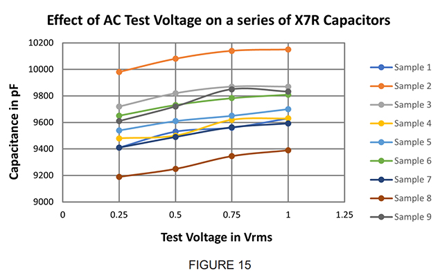
In application, the AC voltage across the chip capacitor may in some cases well exceed the 1.0 ± .02 Vrms test voltage, generating a substantial increase in capacitance. Analogous to the interpretation of DC voltage effects, the thickness of the dielectric in question must be considered, ie: capacitance vs AC voltage data must be reported as ΔC vs Vrms/Mil.
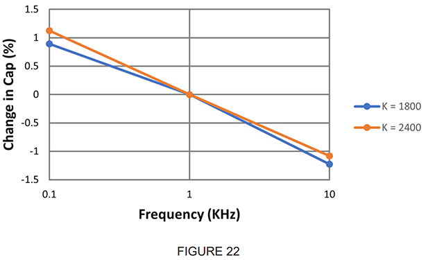
Figure 16 illustrates how the capacitance of various types of Class II dielectrics increases with AC voltage (Vrms/Mil). The capacitance performance vs AC voltage is therefore dependent on the particular design of the chip used.
For example:
1) .01 µF capacitor, K2000 dielectric, with .010” dielectric thickness @ 50 Vrms experiences 5 Vrms/Mil Stress; Capacitance will increase to approximately .012 µF
2) .01 µF capacitor K2000 dielectric with .005” dielectric thickness, @ 50 Vrms experiences 10 Vrms/Mil Stress; Stress; Capacitance will increase to approximately .014 µF
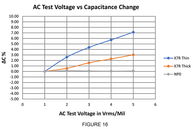
In high AC voltage applications, the manufacturer must design Class II dielectrics to meet the particular needs of the user. Knowledge of the test voltage used by the manufacturer and the operating AC voltage requirements of the customer are therefore important.
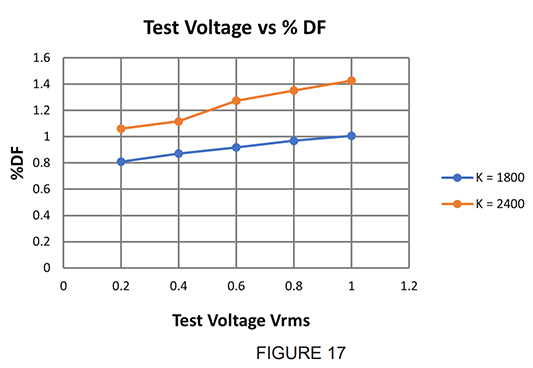
Dissipation Factor and AC Voltage
Class II ceramic dielectrics have a strong dependence of dissipation factor on AC voltage. DF increases with Vrms/ Mil of dielectric. As illustrated in Figure 17, for a series of X7R examples, the change in DF can be considerable with minor variation in test voltage. Curves 1 thru 4 are within specifications @ 1 VRMS (DF<2.5%).
Most manufacturers, including Johanson, test all chips at 1.0 ± 0.2 Vrms standard, as dictated in MIL and EIA specifications. However, some capacitors are available with data based on lower test voltage; users must correlate these data to their requirements for circuit designs based on 1.0 Vrms test data.
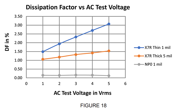
Capacitors of the Class II type operated at high Vrms/Mil will display a considerable increase in dissipation factor, as illustrated in Figure 18, for X7R dielectrics. These chips become quite lossy with as little as 5 Vrms/Mil voltage.
EFFECTS OF DC BIAS:
Capacitance and DC Voltage:
Figure 19 shows typical voltage coefficient data for Class II dielectrics. The section in the text under Electrical Properties, Voltage Coefficient, explains this dielectric behavior.
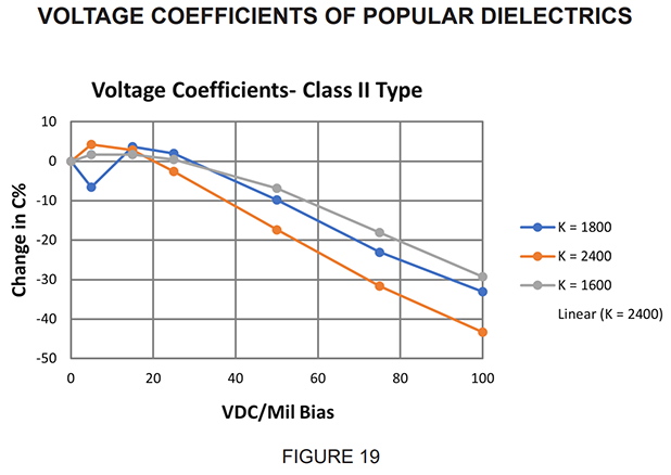
The voltage coefficient is a function of dielectric constant; higher K materials display more radical ΔC with DC bias, due to a higher dependence of K on voltage stress (Figure 20). The dielectric thickness furthermore will determine the volts/mil loading for a capacitor under a given DC voltage bias. The selection of dielectric material and chip design therefore, has strong influence on performance.

BX chips have a temperature voltage coefficient limitation; capacitance cannot drop more than -25% at working bias voltage over the MIL temperature range in most cases -55°C to +25°C. BX design therefore requires a dielectric thickness that limits the volts/mil stress to a % capacitance change, which, when added to the temperature coefficient, does not exceed a net of -25%. This requirement does not apply to the EIA X7R specification. In practice, it is found that for K2000 dielectric, the voltage stress cannot exceed 45 volts/mil (a -20% capacitance change), as the temperature coefficient of this material is typically -5% at the most negative point of the TC curve. High value, higher voltage (>1000 VDCW). Class II dielectrics consequently generally meet X7R specification only, and not BX specification.
A fallacy which exists in the Industry is the use of high K (K >4000) Class II dielectrics at voltages exceeding 5 → 10 volts/mil loading of the capacitor. As is evident in the DC bias graph below, high K dielectrics experience radical decrease of the dielectric constant with DC bias. A K7000 dielectric capacitor, for example, at 50 VDCW, requires a dielectric thickness of at least 10 mils to minimize the voltage coefficient to less than -10% change in capacitance. The buildup of dielectric to such thickness precludes the high volume efficiency of the capacitor. In effect, the “effective” dielectric constant of such a unit is less than what can be achieved using a lower K dielectric with a lesser voltage coefficient.
FREQUENCY EFFECTS:
Capacitance and Frequency:
Ferroelectric dielectrics show strong dependence of dielectric constant on frequency. This behavior arises due to the effect of the alternating field on the polarization mechanisms which give rise to the dielectric constant. In the polarization processes described under Electrical Properties, Dielectric Constant have differing frequency responses. An increase in frequency of the applied field causes some of the polarization mechanisms to lag the field reversals, increasing the loss factor and decreasing the contribution to the net polarization (Figure 21). This change in the polarization is reflected by the dielectric constant and, hence, the capacitance of the ferroelectric dielectrics (Figure 22).
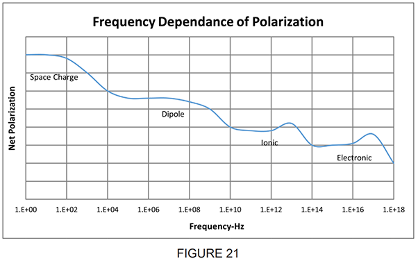
Polarization vs Frequency: (From W.D. Kingery – Introduction To Ceramics)
@ >104 Hz space charge polarization makes no contribution
@ >1010 Hz dipole orientation makes no contribution
@ >1014 Hz ionic polarization makes no contribution – only electronic polarization can keep up with the field reversals, to 10^17 cps.
Dissipation Factor and Frequency:
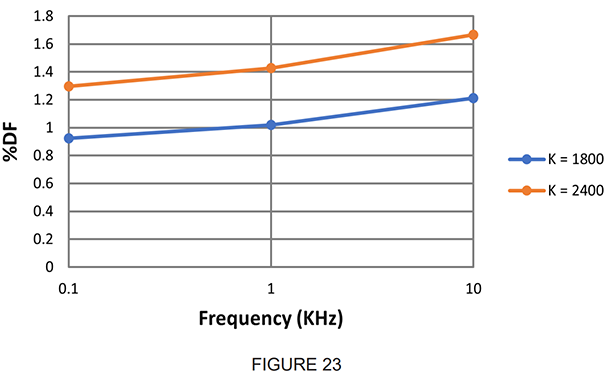
Figure 23 shows DF (Dissipation Factor) data with frequency for typical X7R formulations. Increased loss with frequency occurs due to the inability of the polarization processes to keep pace with the alternating field.
Temperature Dependence
Capacitance and Temperature:
The effect of temperature on capacitance and the calculation for temperature coefficient for Class I and Class II dielectrics is given under Electrical Properties, Temperature Coefficient; the characteristic TC curves for these dielectrics are shown under “Classes of Dielectrics.”
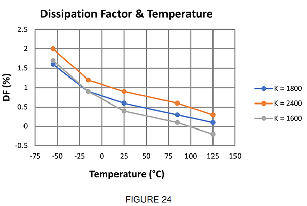
Dissipation Factor and Temperature:
The stable Class I ceramic formulations have negligible dissipation factor change over the standard operating temperature range. Ferroelectric dielectrics exhibit lower loss with increased temperature, as illustrated in Figure 24. Industry specifications require that DF be less than 2.5% at 25°C reference.
MEASUREMENT OF S-PARAMETERS
Most engineers designing circuits at microwave frequencies conduct RF simulations to ensure circuit performance. At Johanson, we have seen that the most reliable and predictable simulation to prototype results come from the use of measured S-parameters. As such, Johanson gathers measured S-parameters on most RF microwave products.
In today’s measurement world, it is known there are various methods and features which allow DUT de-embedding. Although these methods are known to work well, they still lack the detailed traceability on ‘how’ the system was calibrated due the sensitivity of their sophisticated algorithms and intellectual property. Some also lack compensating for the relationship between the calibration elements and the fixture. Other methods are simply overly theoretical, hence the data generated is not much use on a modern PCB simulation/model. Due to these unknowns, Johanson chose to use the industry proven TRL (thru-reflected-line) calibration system. This is one of the most useful calibration techniques that can yield accurate measurements solely on the DUT & PCB interaction with less effort than most alternative de-embedding systems.
Thru-reflected-line is a pre-measurement error correction that is primarily used in non-coaxial environments, such as waveguide testing, using test fixtures or making on-wafer measurement with probes. -Keysight “Stripline TRL Calibration Fixtures for 10-Gigabit Interconnect Analysis.”
HIGH RELIABILITY TESTING
The monolithic, impervious, inorganic structure of ceramic chip capacitors has created a new generation of high reliability components. High reliability testing is often performed to qualify capacitors to MIL-STD 202 (Method 108), Life Test requirements, or to customer specifications.
High reliability testing performed at elevated temperature and working or higher voltage, for a specified time period (often referred to as “burn-in”), is used to establish criteria for two basic purposes:
a) Life Test: Determination of failure rate (loss of capacitance, insulation resistance, DF or mechanical degradation).
OR…
b) Voltage conditioning: Determination of capacitance change (accelerated ageing- Class II dielectrics), and effect on IR and DF.
High reliability testing of Class I stable dielectrics poses no particular problem in interpretation of the test data, as these materials do not age with time, temperature, and voltage, as occurs with Class II dielectrics. High reliability data for Class II dielectrics requires definition of the capacitance change after testing, as two situations must be considered:
a) Chips are tested after accelerated ageing, and a loss of capacitance is reported.
b) Chips are allowed to de-age after Life Test, and no substantial change in capacitance is reported.
Table V illustrates how removal of DC bias at discrete times in the cooling cycle after Life Test affects the capacitance readings of Class II dielectrics. Customer and manufacturers must correlate the requirements and test procedures; the following general considerations apply:
a) Customers desiring “stabilization” of Class II chips require aged capacitors. A change in capacitance tolerance must be tolerated between pre-test and post-test readings, as all high k ferroelectric dielectric age. The manufacturer must select chips which age into the desired capacitance range. Users cannot attach chips with bonding methods that expose the units to temperatures exceeding the Curie point of the dielectric, as this causes de-ageing, and a consequent loss of the stability attained in the voltage-conditioning or life testing.
b) Life test reliability for Class II dielectrics allows limited degradation of DF, IR, or capacitance after Life Test. De-ageing of chips, however, is necessary to obtain meaningful data, as the ferroelectric ceramic age under these test conditions. Life reliability is verified only if de-aged units regain full capacitance after test.
TABLE V
AGEING EFFECTS IN LIFE TESTING
| Group | Initial Check (De-aged) |
Bias Removal Parameters |
Life Test Results |
||
|---|---|---|---|---|---|
| Capacitance | DF | Capacitance | DF | ||
| I | .127 μF | 0.8% | Cooled for 85°C to 25°C with bias applied | .070 | 0.4% |
| II | .126 μF | 0.8% | Bias off at 85°C hold 2 hrs @ 85°C, cooled to 25°C |
.084 | 0.4% |
| III | .117 μF | 0.8% | Bias off at 85°C, heat to 125°C for 2 hrs, cool to 25°C |
.120 | 0.8% |
Group I: Units are not allowed to de-age, as bias is maintained through the cooling cycle. Group II: Units do not age, as Group I units, as bias is removed well before cooling cycle begins. Group III: Units de-age fully, due to 125°C environment with no DC bias.
GENERAL TESTING & QUALITY CONFORMANCE REQUIREMENTS
Other quality conformance requirements may be applicable to chip capacitor performance, such as solderability, thermal shock, and immersion resistance, fungus and moisture resistance. Table VI lists all relevant electrical and quality specifications applicable to multilayer ceramic capacitors.
TABLE VI
CHIP CAPACITOR SPECIFICATIONS
Electrical Tests: MIL-PRF-55681
MIL-STD-202
Test Methods for Electronic & Electrical Component Parts Method 305 Capacitance, Dissipation Factor. Method 302 Insulation Resistance Method 301 Dielectric Withstanding Voltage
Quality Conformance Tests: MIL-PRF-55681
MIL-STD-202
Test Methods for Electronic & Electrical Component Parts Method 208 Solderability Method 107 Thermal Shock Method 106 Moisture Resistance Method 508 Fungus Resistance Method 104 Immersion
Reliability Conformance Tests: MIL-PRF-55681
MIL-STD-202
Test Methods for Electronic & Electrical Component Parts Method 108 Life Test
EIA Standard RS-198 = General Specification for Ceramic Dielectric Capacitors
SOME ANSWERS ON CHIPS
Geometry
Johanson Technology and Johanson Dielectrics manufacture capacitors with maximum volume efficiency of capacitance. Chip design and ceramic tape processing methods allow for high layered construction with thin dielectric and narrow margins. Maximum efficiency is attained using high k dielectrics and optimum design; low voltage high k chips are manufactured exceeding 1500 µF/in3 volume efficiency.
Capacitor design (dielectric thickness, number of layers, and cover layer thickness) is selected for any requirement by a computer, which is programmed to calculate the best design for the electrical parameters required (capacitance, working voltage, dielectric withstanding voltage, and I.R.).
Chips are built in various sizes and configurations to suit user demand. Configurations include circular feed-thru and multi-feed-thrus as well as standard chips. Sizes vary from .040” x .020” (L x W) to approximately 1.480” x 0.790” for the larger units. Standardization sized to EIA recommended dimensions is now occurring in the industry.
The Johanson catalog illustrates typical capacitor configurations.
Terminations
Electrodes are given a common terminal by coating the chip ends with a precious metal-glass formulation suspended in an organic vehicle. Consequent drying and firing eliminates the organic components and affects a bond between the ceramic dielectric and glass constituent in the termination. Most common termination materials include Palladium-Silver alloy, Silver, and Gold.
The quality of chip termination is based on the following criteria:
a) Coverage c) Solderability b) Strength d) Leach Resistance
a and b above are both functions of termination processing: Proper coverage is dependent on dipping method, rheology of termination suspension, and wetting characteristics (surface energy relationship of termination to ceramic).
Termination strength is dependent on quality of coverage, firing history, and glass frit constituents. The glass frit is selected to be compatible in thermal expansion to the ceramic dielectric to preclude the development of undesirable stresses between chip and bond during processing.
In addition to the soldering process itself, solderability of the termination is dependent on the termination material. Excessive firing of the termination causes migration of glass to termination surface, precluding good solderability. Leach resistance is a function of the metal or metal alloy in the termination and the solder composition and process used.
Capacitor Attachment
Chip attachment to substrate pads can be performed in a variety of methods:
A) Soldering:
1) Dipping: Chip terminations and substrate pads are pretinned. Chip and substrate are heated gradually to effect solder flow and bonding. Temperature required is a function of solder type – generally 400 - 500°F.
2) Paste/Preforms: Solder paste is applied to the substrate by screening or preform method. Chip and substrate are heated to effect solder flow and bonding. Temperature required is a function of solder type generally 500-600°F.
B) Ultrasonic Bonding
This is a cold bonding method adaptable to the joining of dissimilar metals and sections of different thicknesses. Ultrasonic bonds are produced by applying pressure to the surfaces to be joined by a transducer tip vibrating at about 60 KHz. The force of the scrubbing action causes molecular mingling of the surfaces in contact, thereby forming a bond.
Some type of preform material is usually placed between the chip and conductor interface.
C) Thermo-Compression Bonding:
This is a heat/ pressure bonding technique. The chip is pressed onto a heated substrate, in the same manner that semiconductor dice are attached. A preform material, such as AuSn, may be used at the substrate chip interface. Required temperature in the range of 375-400°C.
D) Conductive Epoxy
Chips are attached to substrate pads using a conductive epoxy bond between pad and chip termination. Temperature required varies from room to 300°F, depending on epoxy type.
E) Non-Conductive Epoxy
Chips are located and bonded onto the substrate with epoxy. Electrical connection is completed using secondary gold or aluminum wire bonding methods. Epoxy bond temperatures vary from room to 300°F.
The recommended techniques for a given capacitor termination and conductor metallization materials are shown in Table VII.
Table VII
RECOMMENDED CAPACITOR ATTATCHING
| Substrate Conductor Metallization |
Capacitor Termination Material | |||
| Palladium Silver |
Gold | Silver | Recommended Capacitor Termination |
|
| Gold (Evap.) Thin Film |
DE | BCDE | BCDE | Gold |
| Gold (Plated) | ADE | BDCE | BCADE | Gold |
| Platinum-Gold | ADE | BDCE | ACBDE | Palladium-Ag |
| Silver | AD | BCD | ABCD | Pd/Ag or Ag |
| Palladium-Silver | AD | D | AD | Pd/Ag |
| Aluminum (Evap.) | DE | DE | DE | Gold |
↓ |
||||
| These letters apply to the preceding paragraphs. Examples below. |
||||
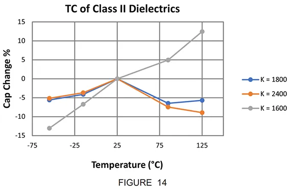
Typical temperature characteristics of Mid an High dielectrics are shown in Figure 14.
DE = Conductive Epoxy, Non-Conductive Epoxy
BCDE = Ultrasonic Bonding, Thermo-Compression Bonding, Conductive Epoxy, Non-Conductive Epoxy
Thermal Cycling
Chip capacitors have thermal properties characteristic ceramic materials. Originally processed at high temperature, chips can withstand exposure to temperatures limited only by the termination material (which is processed at approximately 800°C).
Of importance is the rate at which chips are cycled through temperature changes. Chips, as with all ceramics, are stronger under compressive than under tensile forces. When heating a capacitor, it expands, creating a compressive state of stress; on cooling, the chip contracts, generating a tensile state of stress. The degree of stress developed in thermal cycling is dependent on the coefficient of expansion of the dielectric, and the temperature gradient experienced by the chip (change in temperature and rate of change).
Ceramic dielectrics typically have expansion coefficients ranging from approximately 9.7 X 10⁻⁶ (in/in/)°C to 12.2 X 10⁻⁶ (in/in)/°C, (RT to 300°C), depending on dielectric composition. This expansion coefficient range is high enough to require control of the temperature gradient experienced by chips in thermal processes (such as bonding) to minimize thermal shock hazards. The following general recommendations apply:
a) The rate of cooling is critical, as the chip is under a tensile state of stress. Too rapid of a cooling rate creates a temperature gradient across the chip cross-section which, if too severe, will induce tensile stresses which overcome the intrinsic strength of the chip, resulting in failure.
b) The rate of heating is not as critical, as long as the chip is heated uniformly. Under these conditions, the entire chip is under compressive stress. Non-uniform heating creates a thermal gradient across the chip; the hot portion wants to expand, yet is restrained by the cold portion, generating undesirable tensile stress. Similarly, too fast a heat rate creates non-uniformity between the interior and surface of the chip. Pre-heating of units to intermediate temperature before thermal processing is recommended.
c) Larger units are more prone to thermal shock than smaller units as increased mass can develop more severe thermal gradients for any given rate of temperature change.
d) Leads attached to chips or other heat sinks create localized cooling of the chip surface, generating temperature gradients and tensile forces which may result in a failure. Chips in contact with heat sinks must be cooled in a controlled environment to eliminate thermal shock failure.
Thermal shock failure is often not easily detectable. Chips develop micro-cracks which are not discernible, unless viewed at high magnification, or made visible by coating with a dye. Electrically, an increase in dissipation factor generally occurs with thermal shocked units.
Piezoelectric Properties
Dielectrics possess high dielectric constant due to the displacement of ions under the influence of an electric field. In Ti02, for example, the contribution to polarization occurs due to a displacement of the Ti atom. This displacement, in turn, is partly compensated for by a constriction of other atoms, causing an elastic deformation, termed “electrostriction.” Electrostriction is manifested in all dielectric solids. Materials based on ferroelectric materials, such as BaTi03, display reciprocity between an applied field and mechanical deformation, and are termed “piezoelectric.” These are materials, which, in addition to displaying electrostrictive behavior, also polarize under applied pressure. Piezoelectricity is therefore an electro-mechanical coupling. The strain induced by an electric field is proportional to the applied field. Conversely, the induced field intensity or polarization is proportional to the applied stress. Piezoelectricity is characteristic of all materials which do not possess a center of symmetry in the crystal atomic arrangement. Class I dielectrics display electrostriction, but are not piezoelectrics, as the crystal lattice of the ceramic used in these dielectrics possesses a center of symmetry. In short, an applied field causes elastic deformation; applied stress, however, does not induce field intensity.
PARAMETERS TO CONSIDER IN SELECTING CAPACITORS
Selection of chips and dielectric for any application is based on the following considerations:
a) Temperature Stability (TC):
Capacitance stability required over the operating temperature range dictates dielectric type.
b) Voltage-Temperature Coefficient:
Capacitance stability within a given tolerance over the temperature range with working voltage further specifies dielectric and chip design requirements.
Example: ΔC to be ± 15%, -55 to 125°C: X7R characteristic
ΔC to be -25+15%, -55 to 125°C @ VDCW = BX characteristics
Chips must be designed to control operating volts/mil to meet these characteristics
c) Capacitance / Size:
Capacitance value required dictates chip size. Chip size is also dependent on working voltage and dielectric withstanding voltage requirements, which determine dielectric layer thickness.
d) Capacitance-Tolerance:
Tolerance required determines design of chip and dielectric used. Example: Close tolerances (< ± 5%) require use of stable Class I dielectrics. Ferroelectric dielectrics, which exhibit strong dependence of capacitance on time and temperature cannot be meaningfully sorted into close tolerance. Mid K dielectrics (stable Class II) are sufficiently stable to sort into ±10% and larger tolerance. ± 5% tolerance is possible, but users should remember the ageing factor and temperature dependence of these dielectrics.
A ± 5% tolerance may be exceeded when bonding of chips to substrate if temperatures above the Curie point of the dielectric are experienced, due to the de-ageing phenomenon.
High K dielectrics are not sufficiently stable to sort into capacitance tolerances less than ±20%. These chips are usually sold with +100 or +80% tolerances, due to the very strong temperature and time -0 -20 dependence of capacitance.
e) Operating and Dielectric Withstanding Voltage:
This requirement dictates thickness of the dielectric layer, and consequently influences chip size. Voltage can also restrict dielectric type if voltage sensitive high k dielectrics are required to meet capacitance value. Example Z5U can be used to manufacture 12 volt 1.0 µF chips. At 50 VDCW requirement, voltage derating can be as much as 80%, depending on chip size & dielectric layer thickness, precluding use of this dielectric at 50 VDCW.
f) Q Factor:
The quality factor required dictates type of dielectric material:
Q >10,000 (a) 1 MHz = Hi-Q dielectric Q >1000 (a) 1 MHz = NP0 dielectric
g) Termination:
Standard termination materials and solder are available for any type of capacitor.
h) Overdesign-Safety Margin:
Johanson as all chip manufacturers, incorporates a safety margin into the design of chips, to minimize potential failures in chip production and use. Specifications for chip capacitors usually include a built-in safety margin. It often occurs that, along the entire sequence of events between the original requirement and the final chip, the units become over-designed to the point where costs and yields are affected. Delivery and costs are optimized when an understanding of true chip requirements and reasonable safety margins are reached.
RELEVANT MILITARY STANDARDS CAPACITORS
- MIL-PRF-20
- Title: Capacitor, Fixed, Ceramic Dielectric (Temperature Compensating), Established Reliability and Non-Established Reliability, General Specification for
- Applicable Products: Leaded MLCCs
- Common Applications: Used when established reliability levels are a requirement (Space)
- MIL-PRF-123
- Title: Capacitors, Fixed, Ceramic Dielectric, (Temperature Stable and General Purpose), High
Reliability, General Specification for
- Applicable Products: Leaded and Non-Leaded MLCCs
- Common Applications: Used when established reliability levels are a requirement (Space)
- MIL-PRF-15733
- Title: Filters and Capacitors, Radio Frequency Interference, General Specification for
▪ Applicable Products: Feed-Thru Filters
- Common Applications: For Low-Pass Filters and Capacitors to suppress FR/EM interference
- MIL-PRF-28861
- Title: Filters and Capacitors, Radio Frequency/Electromagnetic Interference Suppression,
General Specification for
- Applicable Products: Discoidal Capacitors
- Common Applications: Pi Filters in Connectors
- MIL-PRF-31033
- Title: Capacitors, Fixed, Ceramic Dielectric, High Reliability, Discoidal, General Specification for
- Applicable Products: Discoidal Capacitors
- Common Applications: Intended for RFI/EMI suppression filters covered by MIL- PRF- 28861
- MIL-PRF-32535
- Title: Capacitor, Chip, Fixed, Ceramic Dielectric (Temperature Stable and General Purpose),
Extended Range, High Reliability and Standard Reliability, General Specification for
- Applicable Products: MLCCs
- Common Applications: BME and PME options and for higher capacitance values than MIL-PRF-123 and MIL-PRF-55681 for a given size and voltage
- MIL-PRF-39014
- Title: Capacitor, Fixed, Ceramic Dielectric (General Purpose) Established Reliability and Non-established Reliability General Specification for
- Applicable Products: Leaded MLCCs
- Common Applications: Use for more stringent acceleration factors
- MIL-PRF-49464
- Title: Military Specification, Capacitors, Chip, Single Layer, Fixed, Parallel Plate, Ceramic Dielectric. Established Reliability, General Specification for
- Applicable Products: Single Layer Ceramic Capacitors
- Common Applications: General requirements for ceramic parallel plate, Single Layer Capacitors
- MIL-PRF-49467
- Title: Capacitor, Fixed, Ceramic, Multilayer, High Voltage (General Purpose), General
Specification for
- Applicable Products: High Voltage MLCCs
- Common Applications: General requirements for ceramic Multilayer High Voltage Capacitors
- MIL-PRF-49470
- Title: Capacitor, Fixed, Ceramic Dielectric, Switch Mode Power Supply (General Purpose and Temperature Stable), General Specification for
- Applicable Products: SMPS Leaded MLCCs
- Common Applications: General requirements for general purpose (BQ, BR, and BX characteristics) and temperature stable (BP characteristic) ceramic capacitors for use in switch mode power supplies.
- MIL-PRF-55681
- Title: Capacitor, Chip, Multiple Layer, Fixed, Ceramic Dielectric, Established Reliability and Non-Established Reliability, General Specification for
- Applicable Products: High-Q/Low Loss high frequency MLCCs
- Common Applications: Widely used for high frequency applications