Antenna Tuning & Layout Techniques
Outline
- Chip Antenna Characteristics
- Antenna Selection Considerations
- Circuit Design Constraints
- Layout Tips
Motivation
Chip Antenna an efficient means of “connectivity” to modern portable compact electronic devices.
Miniature portable devices requires small antennas.
Can be internalized – i.e. “Concealed” within device.
Pros & Cons
Pros:
- Chip antennas are small, cheap and performs well.
- Bulky external “whip” type antennas are thing of the past.
Cons:
- Must be accounted for during initial circuit design stage.
- Interference, proximity de-tuning & degradation concerns.
Ultimate Goal is to Maximize Performance
LTCC Chip Antennas
Chip Antenna Characteristics - 1
- Features Ag radiating element encapsulated in ceramic.
- A quarter-wave (λ/4) monopole system.
- Works with GND plane to form dipole system.
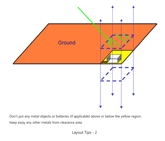
- Certain “No-GND” metal-free space necessary.
- Small form factor, thin profile & light weight.
Chip Antenna Characteristics - 2
- Omni-directional radiation.
- Linear Polarization.
- Mounting configuration flexibility.
- Frequency range supported: 0.08 GHz thru 10 GHz.
- WiFi, BT, WiMAX, UWB, GSM, CDMA, GPS etc.
- Suitable for Pick & Place.
Antenna Selection Considerations
Considerations - 1
- Size
- Frequency Band
- Bandwidth
- Polarization
- Peak Gain
- Average Gain
- Radiation Pattern requirements
Considerations - 2
- Successful Antenna design means harmonious interaction of the “seven” parameters (next page).
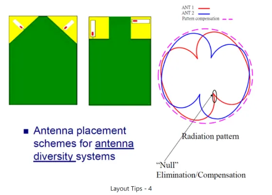
- Additional considerations for diversity systems – e.g. MIMO
- Overall performance is always system dependent.
Circuit Design Constraints
- Size of the Circuit board.
- Layout of other board components.
- Complexity of circuit.
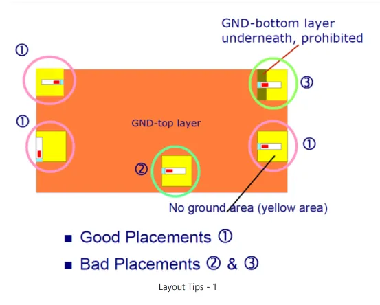
- Proper GND/No-GND dimensions and clearances.
- “Tuning” Matching Circuitry
- Shielding
- Suitable Enclosure (material)
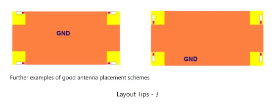
Layout Tips
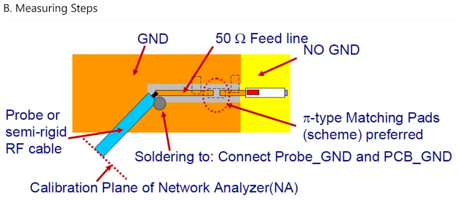
A. Antenna Matching Setup
1. One-port (S11) calibration for N.A. (Network Analyzer) Open-Short-Load for desired operating bandwidth
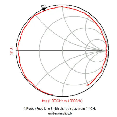
2. Mount probe (semi-rigid RF cable for our example) onto PCB and connect to N.A.
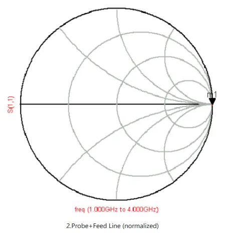
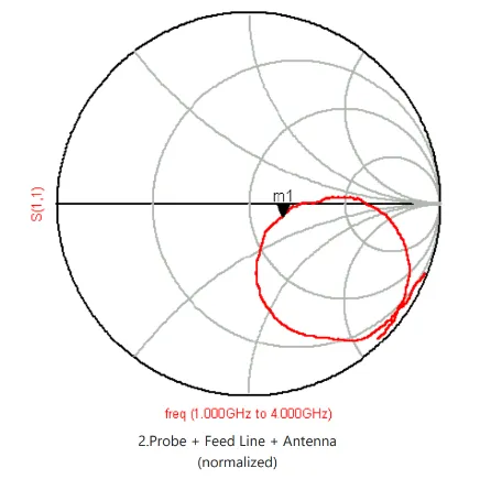
3. Measure S11 of test board without antenna or any matching components and save as: →S11_open →save trace to memory of N.A.
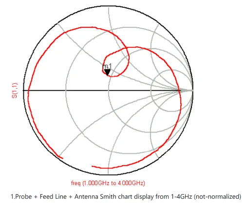
4. Measure S11 of test board with antenna and series 0Ω resistor mounted and save as: →S11_antenna
5. Set N.A. to data/memory mode (S11_antenna/S11_open) and display/save as: →S11_match
6. Match the trace of S11_match to 50Ω (center of Smith chart at the desired frequency)
| Part Number | 2450AT45A100 |
|---|---|
| Frequency Range | 2400 - 2500 Mhz |
| Peak Gain | 3.0 dBi typ. (XZ-V) |
| Average Gain | 1.0 dBi typ. (XZ-V) |
| Return Loss | 9.5 dB min. |
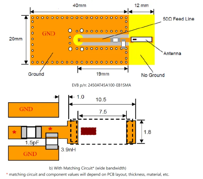
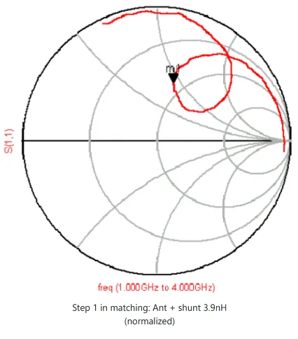
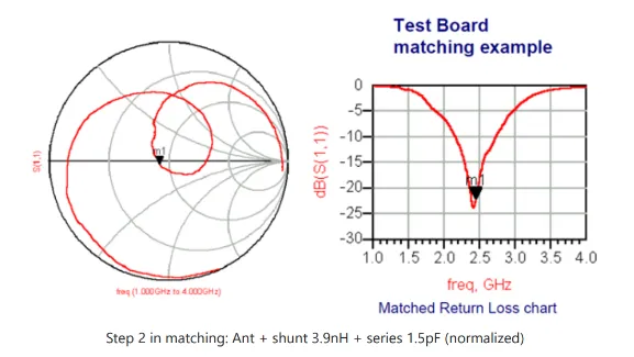
JTI P/N for Matching Circuit: Cap (1.5pF): 500R07S1R5BV4T Inductor (3.9nH): L-07C3N9SV6T