Designing for EMC Flexibility with Multi-Function EMI Filters
How the Proactive EMC Layout Strategy Works
Reserve the location during PCB layout. Measure the EMI problem. Select the filter response from measured evidence. Populate and retest.
A proactive EMC layout strategy reserves an unpopulated Multi-Function EMI Filter footprint at a likely noise source or coupling path before the final filter response is known. The baseline circuit remains electrically continuous. After pre-compliance testing identifies an offending frequency and current path, engineers can select a frequency-characterized filter, populate the reserved location, and retest the same PCB.
Core principle: Separate the PCB-layout decision from the final part-number decision. Establish a usable noise-mitigation location during layout, then select and populate the filter after measurements identify the problem frequency and current path.
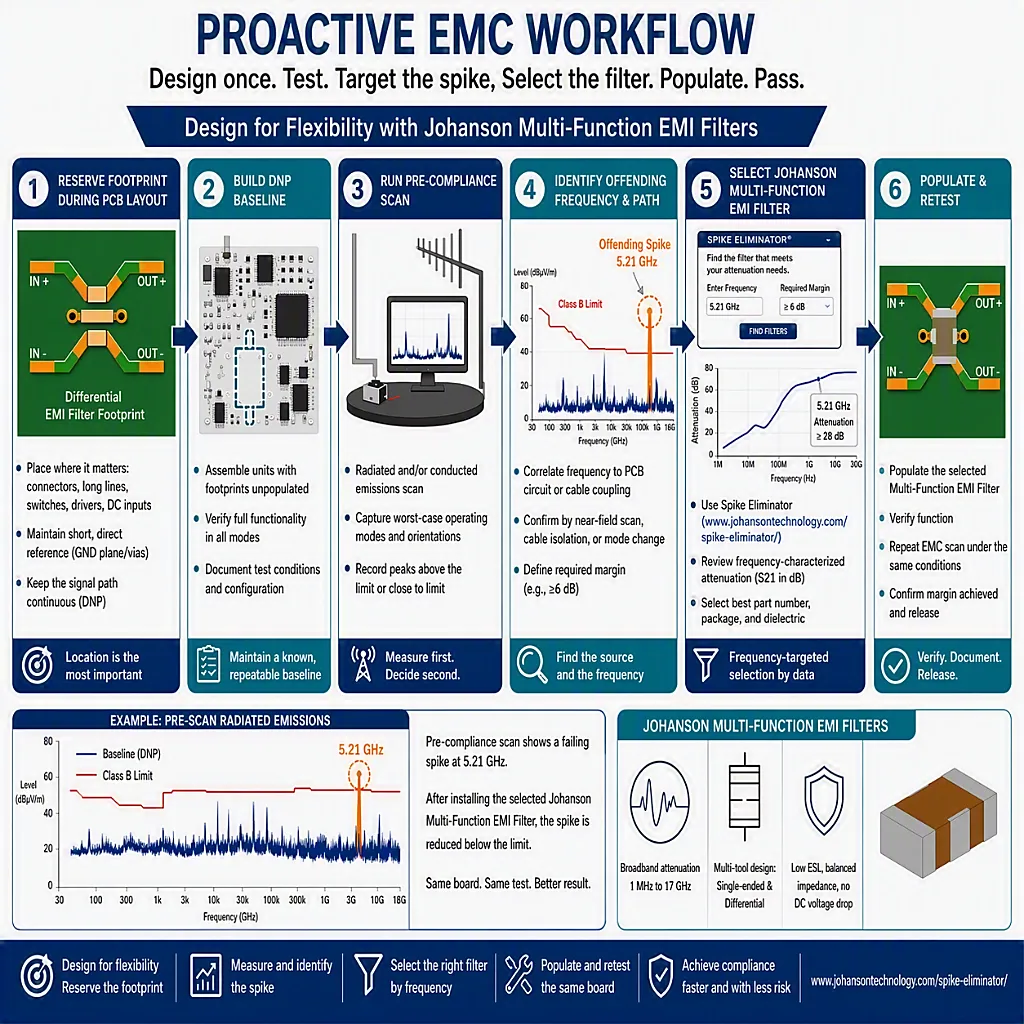
Figure 1. Simplified proactive EMC workflow: reserve, measure, identify, select, populate, and retest.
Key Takeaways
- Reserve a production-ready filter footprint while the PCB is being laid out, even when the final filter part number is not yet known.
- Keep the baseline signal or power path continuous when the reserved component is designated do not populate (DNP).
- Measure the assembled system before selecting the final attenuation response.
- Identify both the offending frequency and the path carrying the unwanted RF current.
- Select candidates using measured attenuation-versus-frequency data and actual electrical, mechanical, environmental, and qualification constraints.
- Verify normal operation and repeat EMC testing after the filter is populated.
- Treat component characterization as a selection tool, not proof of installed-system compliance.
Why the Final EMI Filter Is Often Unknown During PCB Layout
During schematic capture and PCB layout, an engineer may identify a connector, power rail, motor lead, LED cable, long trace, or differential pair as a potential EMC path. However, the frequency that ultimately creates an emissions problem may not be known until the assembled product undergoes pre-compliance or formal EMC testing.
Why schematic-level predictions may be insufficient
- Compliance testing evaluates the assembled product rather than an isolated schematic block.
- Cables, enclosure hardware, grounding, loading, orientation, and operating mode can change radiated and conducted emissions.
- A measured emissions peak may be associated with a higher-order harmonic rather than the fundamental switching or signaling frequency.
- Component attenuation data can narrow the candidate set, but the complete PCB and system must be verified by retest.
Design implication: Delay only the response-selection decision. Do not delay the mechanical location and RF-current-path decision, which can be difficult to recover after routing is complete.
What Is a Multi-Function EMI Filter?
A Johanson Multi-Function EMI Filter is an integrated passive component designed to suppress unwanted electromagnetic energy in single-ended or differential configurations. The portfolio described in the source paper includes EIA case sizes from 0402 through 1812 and frequency-characterized attenuation responses extending from approximately 100 kHz to 18 GHz, depending on the individual part number and frequency.
Relevant filter characteristics
| Attribute | Design relevance |
|---|---|
| Single-ended and differential configurations | Supports power, signal, and balanced-pair mitigation when the PCB is laid out for the intended configuration. |
| Frequency-characterized response | Allows candidates to be evaluated at a measured problem frequency instead of being selected only by nominal capacitance. |
| Ultra-low ESL | Supports high-frequency filtering when low-inductance mounting and reference connections are maintained. |
| No DC voltage drop | Supports DC and signal paths where series voltage drop is undesirable. |
| No series-winding current-rating constraint | Avoids the series-winding current-rating constraint associated with some filtering approaches. Confirm all applicable product and system limits. |
Selection boundary: Portfolio-level frequency ranges do not predict attenuation in a specific installed system. Review the characterized response for the individual part, confirm voltage, package, configuration, dielectric, temperature, and qualification requirements, and retest the populated product.
How the Proactive EMC Strategy Works
Design for optionality
Reserve filter footprints at likely EMI sources, board boundaries, connectors, long routes, switching circuits, motor wiring, LED wiring, and differential interfaces. Preserve short reference paths and differential-pair symmetry.
Measure the assembled system
Record the emissions frequency, measured level, applicable limit, required reduction, operating mode, load, orientation, cable configuration, and other relevant test conditions. Use controlled diagnostic changes to connect the measured frequency to a likely source and coupling path.
Implement from measured evidence
Compare filters that fit the reserved footprint and satisfy the electrical and qualification requirements. Populate the selected candidate, verify normal operation, repeat the EMC measurement, and place the final configuration under documented release control.
Eight-Step Proactive EMC Development Workflow
The six-panel graphic is a simplified visual summary. The following eight-step method is the complete technical workflow.
1. Map likely RF-current paths
Identify external cables, connectors, long traces, fast-switching power stages, motor and LED wiring, clocked interfaces, and differential pairs. Prioritize paths capable of carrying high-frequency current to an efficient radiating or receiving structure.
2. Reserve production-ready footprints
Place an appropriate EIA land pattern directly in the targeted signal or power path. Designate the footprint DNP for the initial assembly.
3. Establish a controlled DNP baseline
Confirm that the unpopulated build remains electrically continuous. Record the assembly variant, firmware, loads, cables, operating modes, and test configuration.
4. Run pre-compliance measurements
Measure conducted and/or radiated emissions under the operating modes and orientations required by the compliance plan. Record the frequency, amplitude, applicable limit, and required reduction.
5. Correlate the frequency to its source and path
Use near-field probing, cable isolation, operating-mode changes, load changes, or source disabling to investigate where the unwanted RF current originates and how the current reaches the measured structure.
6. Select candidates using measured frequency and constraints
Compare frequency-characterized parts that fit the reserved footprint. Confirm working voltage, case size, configuration, dielectric, temperature, and qualification requirements. Select sufficient attenuation margin to justify an engineering trial.
7. Populate, verify, and retest
Install the candidate using the intended production connections. Confirm normal operation and signal integrity, then repeat the diagnostic and applicable EMC measurements under controlled conditions.
8. Release the final configuration
Document the selected part number, populated reference designator, assembly variant, operating conditions, functional results, and EMC results. Release the final configuration to the bill of materials and production documentation.
Where to Reserve EMI Filter Footprints
Single-ended power and signal paths
- Route the selected path directly through the intended signal terminals. Avoid branching from the main route into the reserved footprint.
- Position the footprint near the source when the goal is to prevent high-frequency energy from entering a long PCB trace.
- Position the footprint near a connector, cable, load, or board boundary when that structure is the dominant coupling path.
- Use short, wide reference connections with nearby vias to the intended reference plane.
- Do not leave a parallel copper route that bypasses the populated filter.
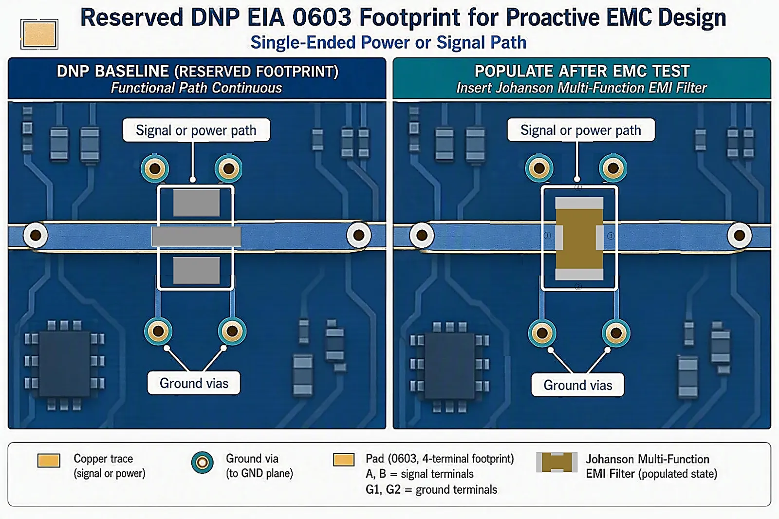
Figure 2. Single-ended EIA 0603 reservation concept. The baseline path remains continuous; the populated state adds short reference connections at the reserved location.
Differential pairs and connector boundaries
- Route both conductors through the intended signal terminals.
- Maintain symmetrical trace geometry through the footprint.
- Preserve matched routing, spacing, reference-plane continuity, and equal via conditions.
- When design constraints justify multiple insertion points, consider reserved footprints near the connector boundary and near the source or receiver.
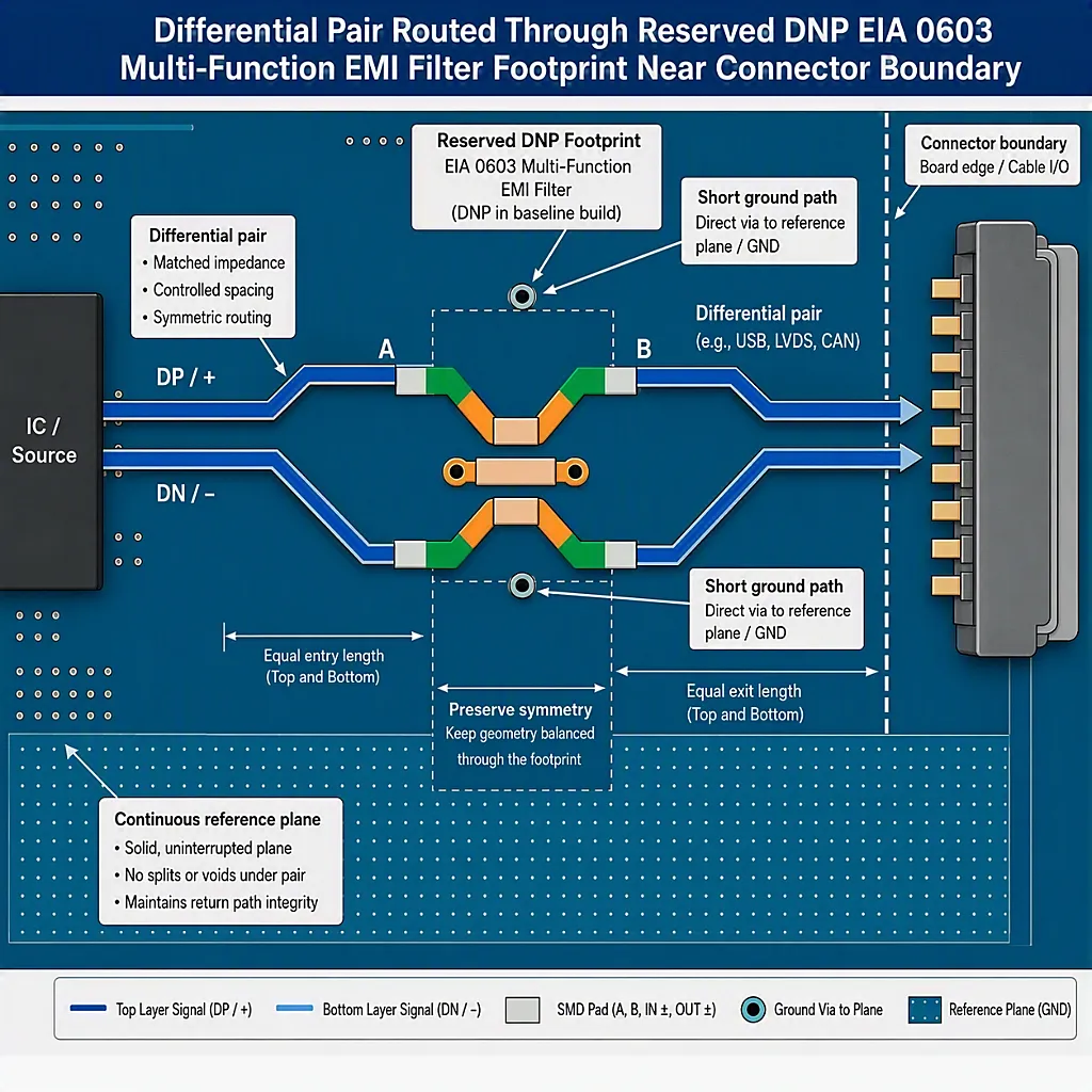
Figure 3. Differential pair routed through a reserved EIA 0603 Multi-Function EMI Filter footprint near a connector boundary.
Recommended Reservation Points by Application
| Application | High-value reservation point | Design rationale |
|---|---|---|
| Cable or connector I/O | Immediately inside the board boundary | Minimizes the unfiltered path connected to an external conductor. |
| Long PCB trace | Source end and, when justified, destination end | Provides alternative insertion points for launched or received high-frequency current. |
| Switching regulator | Appropriate input or output path near the converter | Creates a mitigation point for conducted switching noise without requiring a long rework path. |
| Motor driver | Driver supply or output path and harness connector | Addresses fast switching and long motor wiring as potential coupling paths. |
| LED driver | Driver supply or output path and cable connector | Provides mitigation near the switching source or external wiring. |
| Differential interface | Source, receiver, or connector boundary | Supports noise mitigation while preserving differential-pair symmetry. |
Wireless Sensor Case Study: Reducing a 5.2 GHz Harmonic
EMC problem
A wireless sensor operating with an 868 MHz radio produced a problematic fifth harmonic at approximately 5.2 GHz. The customer identified the DC supply line as the likely coupling path after measurements near the antenna were described as acceptable. Discrete capacitors ranging from 1 pF to 100 pF did not resolve the issue.
Recommended filter
Johanson recommended Multi-Function EMI Filter EFCF500G38451GV001T for placement on the power rail with the reference terminals grounded. The source white paper states that the part provides a minimum attenuation of 30 dB from 2.5 GHz to 8.3 GHz.
Customer-reported result
After the PCB was redesigned to include the recommended filter footprint and the filter was installed, the fifth harmonic was reported at approximately 15 dB below the referenced EN 300 220 limit. Results may vary with the design, PCB layout, mounting, operating mode, and test conditions.
| Case-study element | Documented information |
|---|---|
| Problem | Fifth harmonic near 5.2 GHz exceeded the applicable limit. |
| Likely coupling path | DC supply path. |
| Prior attempts | Discrete capacitors from 1 pF through 100 pF were ineffective. |
| Recommended solution | EFCF500G38451GV001T installed on the power rail with reference terminals grounded. |
| Reported outcome | Fifth harmonic measured approximately 15 dB below the referenced limit after implementation. |
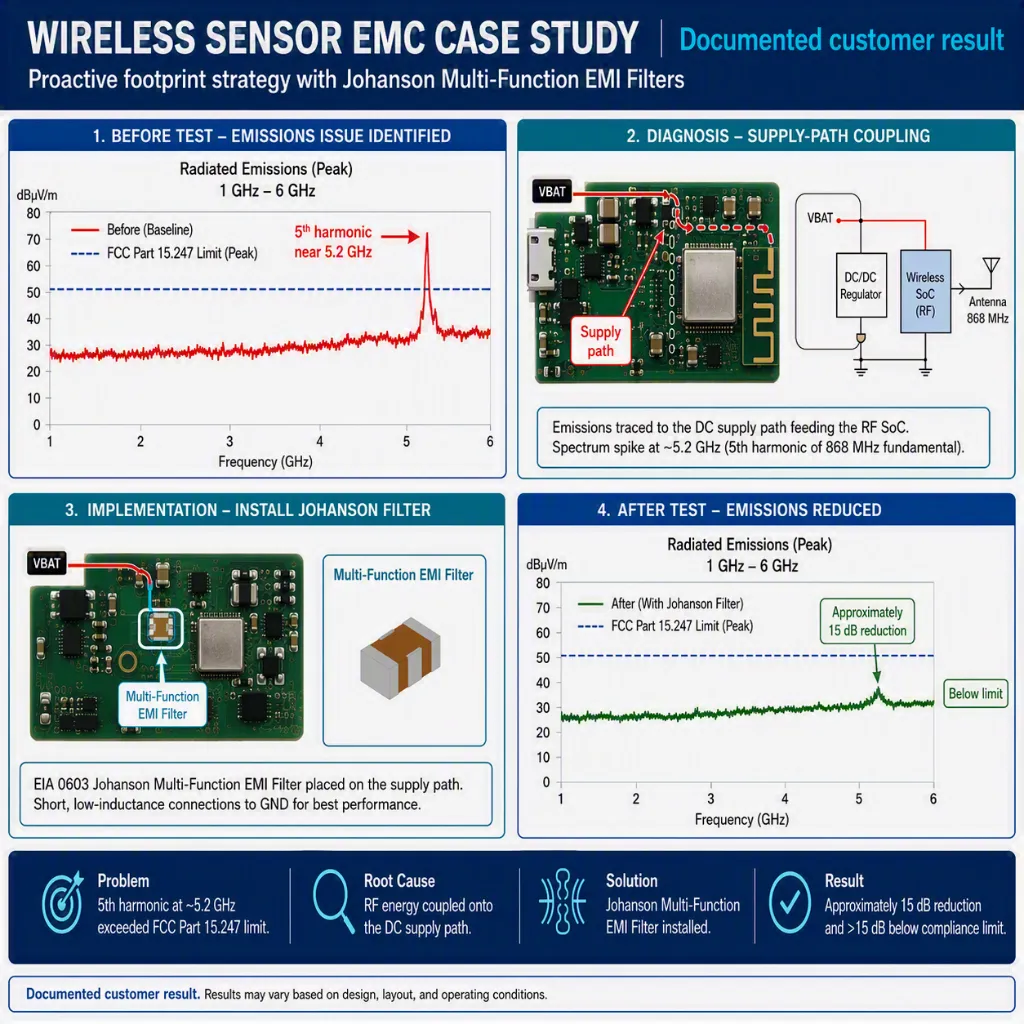
Figure 4. Wireless sensor EMC case study showing baseline emissions, supply-path diagnosis, filter implementation, and the customer-reported retest result.
The missing-footprint cost: The filter addressed the measured problem, but implementation required a PCB redesign to create the footprint. Reserving the footprint during the original layout could preserve a preplanned insertion point and reduce the risk of a layout revision solely to add a filter location.
How to Select a Multi-Function EMI Filter by Frequency
Selection should begin with measured emissions data rather than a guessed capacitance value. Johanson’s Spike Eliminator uses factors including problem frequency, required attenuation, rated voltage, configuration, case size, and qualification to narrow the candidate list.
Information to collect before using Spike Eliminator
- Every relevant emissions spike or affected frequency band
- Measured level at each frequency
- Applicable compliance limit
- Desired engineering margin and required attenuation
- Maximum working voltage
- Single-ended or differential configuration
- Available EIA case size
- Dielectric and temperature requirements
- Commercial or automotive qualification requirements
Candidate-selection rules
- Compare attenuation around every relevant problem frequency.
- Do not select a part only by the deepest attenuation point.
- Constrain results to the land pattern already reserved on the PCB.
- Confirm working voltage and all environmental and qualification requirements.
- Treat the first selected part as an engineering candidate until the complete system passes functional and EMC retesting.
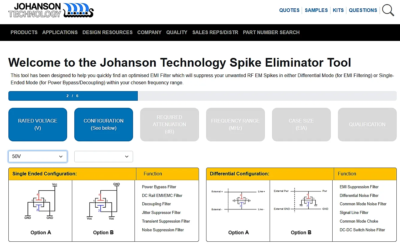
Figure 5. Johanson Technology Spike Eliminator tool.
Use the Spike Eliminator ToolPCB Design and EMC Release Checklist
- Reserved footprints are positioned at likely sources, long routes, cable boundaries, or differential entry and exit points.
- The DNP configuration keeps all intended signal and power paths continuous.
- The land pattern matches the selected EIA case and system-voltage requirements.
- Reference terminals use short, direct, production-ready connections.
- Differential pairs maintain symmetry through the footprint region.
- Test records document frequency, level, limit, margin, mode, orientation, load, and cable configuration.
- Candidate selection reflects the measured frequency and actual package, voltage, configuration, dielectric, and qualification constraints.
- Functional verification and controlled EMC retesting are complete.
- The final part number and assembly variant are released to the bill of materials.
Preferred and Avoided Layout Practices
| Preferred | Avoid |
|---|---|
| Route the targeted path directly through the pads. | Branching from the main route into the footprint. |
| Use short, wide reference connections and nearby vias. | Narrow connections, distant vias, or floating reference terminals. |
| Preserve differential symmetry through the footprint region. | Unequal stubs, bends, via counts, or plane conditions. |
| Document the DNP baseline and populated assembly variant. | Uncontrolled hand rework without configuration records. |
| Compare characterized curves at every problem frequency. | Selecting from nominal capacitance or package alone. |
| Repeat functional and EMC tests after population. | Assuming component data equals installed-system compliance. |
Why reserve an EMI filter footprint before the part number is known?
The final problem frequency may not be known until the assembled product is tested. Reserving a footprint preserves a production-ready mitigation location without requiring the designer to predict the exact attenuation response during the initial PCB layout.
Does a DNP Multi-Function EMI Filter footprint interrupt the circuit?
In the layout method described here, the signal or power path is routed continuously through the footprint region. The baseline assembly therefore remains electrically continuous when the filter is not populated.
Where should an EMI filter footprint be placed?
High-value locations include connectors, cable boundaries, long traces, switching-regulator paths, motor and LED wiring, power rails, and differential interfaces. The correct location depends on the source of the unwanted RF current and the path through which that current couples into a radiating or receiving structure.
How is the required filter attenuation determined?
Required attenuation is derived from the measured emissions level, the applicable limit, and the desired engineering margin. Candidate filters should then be evaluated at every relevant problem frequency.
Can component attenuation data guarantee EMC compliance?
No. Characterized component data helps narrow the candidate list, but the installed PCB and complete product must be functionally verified and retested under controlled EMC conditions.
Why should a filter not be selected only by capacitance?
Nominal capacitance does not show the complete attenuation response across frequency. Frequency-characterized performance is needed to determine whether a candidate provides useful attenuation at the measured problem frequency or frequencies.
Can the same strategy be used for differential signals?
Yes. A differential implementation must route both conductors symmetrically through the intended terminals while preserving pair spacing, matched geometry, reference-plane continuity, and equivalent via conditions.
Reserve the Location First, Select the Response After Testing
The most useful time to create an EMC mitigation location is during PCB layout. The most useful time to choose the final filter response is after the emissions spectrum and coupling path have been measured. A reserved Multi-Function EMI Filter footprint connects those two stages while preserving a production-ready option for later mitigation.
Final design rule: Reserve the appropriate location during PCB layout, select the attenuation response from measured evidence, and verify the populated product under the original controlled EMC conditions.