Multi-Function EMI Filters
Suppress Conducted and Radiated EMI Noise
Reduce common mode noise, differential mode noise, and spurious emissions to improve EMC performance, and system reliability.
- Advanced ceramic filters designed to attenuate unwanted electromagnetic interference (EMI) such as noise (e.g. common mode) or spurious emissions (e.g. CISPR) occurring at a specific range of frequencies.
- Unlike traditional EMI components that rely on series impedance, EF EMI Filter Series operate through a voltage-driven noise filtering mechanism
- These SMD (SMT) passthrough filters can be used in both single ended (e.g. DC source signal) and differential (e.g. +/- signal) applications.
- Effective attenuation from 100KHz to 20GHz with various bandwidths.
- Available in EIA sizes from 0402 (1005 metric) to 1812 (4532 metric) depending on frequency attenuation needs, voltage rating, and feed line geometry.
- Voltages from 10VDC to 500VDC+.
Our EF series EMI filters enable effective suppression of EMI before it propagates through the PCB, cables, or system ground paths, improving overall EMC performance.
Overview
Our multi-functional EMI Filters are designed to attenuate unwanted EM interference (commonly referred to as “noise” or “spurious emissions”) at specific frequencies, allowing DC signals to pass unaltered to critical systems by removing certain unwanted RF signals (voltage noise removal) or filter out transient frequencies. This technology can suppress both common mode and differential noise interference with attenuations of up to 70dB.
Features:
- Our Spike Eliminator Web application will direct you to the specific p/n component that will attenuate your unwanted signal (or group of signals)
- In certain applications these can replace large/expensive/heavy, wirewound (e.g. toroids), bulk electrolytic capacitors, and ferrites.
- Drastically reduces PCB space utilization and BPM count in a cost-effective manner
- DC current path flows straight through the conductor pad and therefore not current limited
- Ultra Low ESL (equivalent series inductance) provides low impedance to ground at high frequencies.
- High reliability with temperature & vibration stability
Benefits:
- Replaces up to 10 discrete capacitive components with 1 EF EMI Filter
- In certain EMI scenarios, these filters can replace or significantly reduce the need for discrete components such as ferrites, wirewound (toroids), or bulk electrolytic capacitors by providing localized targeted noise suppression
- Reduces compliance testing time and cost
- Up to 30% Via Reduction
Applications:
- DC‑DC converters and power supplies
- Military and defense
- Brushless motor drives and industrial automation systems
- PLC I/O and control signal filtering
- FPGA / ASIC / microprocessor power rails
- High-speed digital and RF signal lines
- Automotive electronics and LED drivers
- Wireless charging systems
- Medical electronics
- Aerospace critical systems
- EV systems and battery management
- Industrial and consumer electronics Amplifier Filtering & Decoupling
- High Speed Data Filtering
- EMC I/O Filtering
EMI Spike Eliminator
In most cases, when you have an unwanted spike of RF EM noise, finding the right solution quickly & easily is often difficult. That’s where we can help!
Try our “Spike Eliminator” web tool. Input your “trouble” frequency(ies) and we’ll tell you which of our part numbers are suitable for your application. It’s that simple.
Once you’ve decided on a part number, let us know by submitting a sample request and we’ll send you samples free of charge (up to 20pcs). If you require larger sample quantities, no problem – just click the inventory link and we’ll show you which stocking distributors have stock on hand, ready to ship.
Expert Design Support:
We understand the complexity and difficulty associated with dealing with unwanted EMI issues in your circuit. We have a dedicated team of EMC experts in-house who are ready to support you. Our experienced engineers are here to help solve EMI issues and can support you with:
- Identifying the right p/n component(s) to solve your specific EMI spikes.
- How to design-in and connect Johanson EMI Filters to your product’s schematic to achieve the most effective results.
- Reviewing and optimize your PCB layout, and where required, advise on any necessary changes that can be made to improve EM compliance.
Our goal is to provide you with a solution that will reduce your unwanted EMI noise that enables you to pass the mandatory EMC regulations, so please feel free to contact a member of our team.
Product Range (By Case Size)
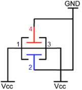
Option A
- Power Bypass Filter
- DC Rail EMI/EMC Filter
- Decoupling Filter
- Jitter Suppressor Filter
- Transient Suppression Filter
- Noise Suppression Filter
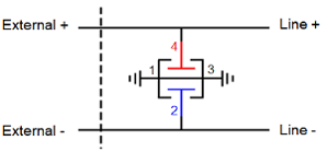
Option A
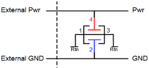
Option B
- EMI Suppression Filter
- Differential Noise Filter
- Common Mode Noise Filter
- Signal Line Filter
- Common Mode Choke
- DC-DC Switch Noise Filter
| Datasheet: Click to Open PDF | Differential Configuration Layout: Download | Single Ended Configuration Layout: Download |
| Rated Voltage | Dielectric | Part Number | Differential Configuration | Single Ended Configuration | Request Samples | Request for Quote | ||||||||||||
|---|---|---|---|---|---|---|---|---|---|---|---|---|---|---|---|---|---|---|
| Typ. 20dB Attenuation Frequency Range (MHz) | Typ. 30dB Attenuation Frequency Range (MHz) | Maximum Attenuation | Attenuation Plot | Typ. 20dB Attenuation Frequency Range (MHz) | Typ. 30dB Attenuation Frequency Range (MHz) | Maximum Attenuation | Attenuation Plot | |||||||||||
| From | To | From | To | dB | MHz | From | To | From | To | dB | MHz | |||||||
| 100 | NP0 | EMCP101G36621GV001T | 3100 | 4200 | 3400 | 3800 | 44.54 | 3600 | Plot | 3700 | 4180 | 3400 | 7400 | 44.54 | 3600 | Plot | Order Samples | Request Quote |
| 100 | NP0 | EMCP101G28471GV001T | 2300 | 3500 | 2600 | 3000 | 45.88 | 2800 | Plot | 2400 | 8500 | 2600 | 5900 | 45.88 | 2800 | Plot | Order Samples | Request Quote |
| 100 | NP0 | EMCP101G17281GV001T | 1200 | 2400 | 1500 | 1900 | 48.66 | 1700 | Plot | 1000 | 7800 | 1500 | 4100 | 48.66 | 1700 | Plot | Order Samples | Request Quote |
| 100 | NP0 | EMCP101G17281GV001T | 1100 | 2200 | 1400 | 1700 | 43.26 | 1500 | Plot | 850 | 7600 | 1400 | 3800 | 43.26 | 1500 | Plot | Order Samples | Request Quote |
| 50 | NP0 | EMCP500G08151GV001T | 470 | 1700 | 710 | 1100 | 56.76 | 880 | Plot | 310 | 7000 | 710 | 2900 | 56.76 | 880 | Plot | Order Samples | Request Quote |
| 100 | NP0 | EMCP101G08151GV001T | 470 | 1700 | 710 | 1100 | 56.76 | 880 | Plot | 310 | 7000 | 710 | 2900 | 56.76 | 880 | Plot | Order Samples | Request Quote |
| 100 | X7R | EMCP101W05061GV001T | 130 | 1900 | 300 | 800 | 36.83 | 500 | Plot | 67 | 7000 | 300 | 2300 | 36.83 | 500 | Plot | Order Samples | Request Quote |
| 100 | X7R | EMCP101W02031GV001T | 29 | 1800 | 83 | 650 | 45.81 | 230 | Plot | 15 | 6800 | 83 | 2200 | 45.81 | 230 | Plot | Order Samples | Request Quote |
| 50 | X7R | EMCP500W01011GV001T | 6.5 | 1800 | 20 | 600 | 52.37 | 110 | Plot | 3.2 | 6800 | 20 | 2200 | 52.37 | 110 | Plot | Order Samples | Request Quote |
| 16 | X7R | EMCP160WD5D61GV001T | 1.4 | 1800 | 4.3 | 570 | 57.33 | 50 | Plot | 0.69 | 6800 | 4.3 | 2200 | 57.33 | 50 | Plot | Order Samples | Request Quote |
| 10 | X7R | EMCP100WD3D41GV001T | 0.64 | 1800 | 2 | 580 | 61.93 | 34 | Plot | 0.32 | 6800 | 2 | 2200 | 61.93 | 34 | Plot | Order Samples | Request Quote |
| 10 | X7R | EMCP100WD2D31GV001T | 0.29 | 1800 | 0.91 | 580 | 65.03 | 23 | Plot | 0.15 | 6800 | 0.91 | 2200 | 65.03 | 23 | Plot | Order Samples | Request Quote |
| Technical Support Contact us for any technical questions | Order Samples Request samples |
| Datasheet: Click to Open PDF | Differential Configuration Layout: Ask a Question | Single Ended Configuration Layout: Download |
| Rated Voltage | Dielectric | Part Number | Differential Configuration | Single Ended Configuration | Request Samples | Request for Quote | ||||||||||||
|---|---|---|---|---|---|---|---|---|---|---|---|---|---|---|---|---|---|---|
| Typ. 20dB Attenuation Frequency Range (MHz) | Typ. 30dB Attenuation Frequency Range (MHz) | Maximum Attenuation | Attenuation Plot | Typ. 20dB Attenuation Frequency Range (MHz) | Typ. 30dB Attenuation Frequency Range (MHz) | Maximum Attenuation | Attenuation Plot | |||||||||||
| From | To | From | To | dB | MHz | From | To | From | To | dB | MHz | |||||||
| 50 | NP0 | EMCF500G63001GV001T | 5800 | 6900 | 6200 | 6500 | 44.04 | 6300 | Plot | 8300 | 14500 | 6200 | 12800 | 44.04 | 6300 | Plot | Order Samples | Request Quote |
| 50 | NP0 | EMCF500G13221GV001T | 850 | 2000 | 1100 | 1500 | 52.10 | 1300 | Plot | 640 | 8000 | 1100 | 3600 | 52.10 | 1300 | Plot | Order Samples | Request Quote |
| 50 | X7R | EMCF500W03041GV001T | 63 | 1900 | 160 | 720 | 42.85 | 340 | Plot | 32 | 7300 | 160 | 2400 | 42.85 | 340 | Plot | Order Samples | Request Quote |
| 16 | X7R | EMCF160W01011GV001T | 6.3 | 1900 | 20 | 600 | 52.37 | 110 | Plot | 3.1 | 7300 | 20 | 2300 | 52.37 | 110 | Plot | Order Samples | Request Quote |
| Technical Support Contact us for any technical questions | Order Samples Request samples |
| Datasheet: Click to Open PDF | Differential Configuration Layout: Download | Single Ended Configuration Layout: Download |
| Rated Voltage | Dielectric | Part Number | Differential Configuration | Single Ended Configuration | Request Samples | Request for Quote | ||||||||||||
|---|---|---|---|---|---|---|---|---|---|---|---|---|---|---|---|---|---|---|
| Typ. 20dB Attenuation Frequency Range (MHz) | Typ. 30dB Attenuation Frequency Range (MHz) | Maximum Attenuation | Attenuation Plot | Typ. 20dB Attenuation Frequency Range (MHz) | Typ. 30dB Attenuation Frequency Range (MHz) | Maximum Attenuation | Attenuation Plot | |||||||||||
| From | To | From | To | dB | MHz | From | To | From | To | dB | MHz | |||||||
| 100 | NP0 | EMCT101G28491GV001E | 2300 | 3500 | 2600 | 3000 | 43.01 | 2800 | Plot | 2400 | 8400 | 2600 | 6200 | 43.01 | 2800 | Plot | Order Samples | Request Quote |
| 100 | NP0 | EMCT101G13231GV001E | 810 | 2000 | 1100 | 1500 | 52.31 | 1300 | Plot | 640 | 8200 | 1100 | 3700 | 52.31 | 1300 | Plot | Order Samples | Request Quote |
| 100 | X7R | EMCT101W07101GV001E | 260 | 2000 | 580 | 900 | 31.73 | 730 | Plot | 150 | 7500 | 580 | 2600 | 31.73 | 730 | Plot | Order Samples | Request Quote |
| 100 | X7R | EMCT101W05071GV001E | 130 | 1900 | 310 | 790 | 35.01 | 500 | Plot | 67 | 7500 | 310 | 2500 | 35.01 | 500 | Plot | Order Samples | Request Quote |
| 100 | X7R | EMCT101W02041GV001E | 43 | 1800 | 120 | 670 | 41.85 | 280 | Plot | 21 | 7400 | 120 | 2400 | 41.85 | 280 | Plot | Order Samples | Request Quote |
| 100 | X7R | EMCT101W01011GV001E | 6.6 | 1800 | 20 | 600 | 52.09 | 110 | Plot | 3.2 | 7400 | 20 | 2400 | 52.09 | 110 | Plot | Order Samples | Request Quote |
| 50 | X7R | EMCT500WD5D71GV001E | 1.4 | 1800 | 4.2 | 570 | 59.02 | 50 | Plot | 0.68 | 7400 | 4.2 | 2400 | 59.02 | 50 | Plot | Order Samples | Request Quote |
| Technical Support Contact us for any technical questions | Order Samples Request samples |
| Datasheet: Click to Open PDF | Differential Configuration Layout: Download | Single Ended Configuration Layout: Download |
| Rated Voltage | Dielectric | Part Number | Differential Configuration | Single Ended Configuration | Request Samples | Request for Quote | ||||||||||||
|---|---|---|---|---|---|---|---|---|---|---|---|---|---|---|---|---|---|---|
| Typ. 20dB Attenuation Frequency Range (MHz) | Typ. 30dB Attenuation Frequency Range (MHz) | Maximum Attenuation | Attenuation Plot | Typ. 20dB Attenuation Frequency Range (MHz) | Typ. 30dB Attenuation Frequency Range (MHz) | Maximum Attenuation | Attenuation Plot | |||||||||||
| From | To | From | To | dB | MHz | From | To | From | To | dB | MHz | |||||||
| 100 | X7R | EMDD101WD8011GV001E | 4.2 | 1800 | 13 | 580 | 56.36 | 89 | Plot | 2.1 | 6500 | 13 | 2100 | 56.36 | 89 | Plot | Order Samples | Request Quote |
| 100 | X7R | EMDD101WD3D41GV001E | 0.64 | 1800 | 2 | 590 | 62.85 | 34 | Plot | 0.32 | 6500 | 2 | 2100 | 62.85 | 34 | Plot | Order Samples | Request Quote |
| 10 | X7R | EMDD100WD1D21GV001E | 0.14 | 1800 | 0.43 | 570 | 66.37 | 16 | Plot | 0.07 | 6500 | 0.43 | 2100 | 66.37 | 16 | Plot | Order Samples | Request Quote |
| Technical Support Contact us for any technical questions | Order Samples Request samples |
| Datasheet: Click to Open PDF | Differential Configuration Layout: Ask a Question | Single Ended Configuration Layout: Ask a Question |
| Rated Voltage | Dielectric | Part Number | Differential Configuration | Single Ended Configuration | Request Samples | Request for Quote | ||||||||||||
|---|---|---|---|---|---|---|---|---|---|---|---|---|---|---|---|---|---|---|
| Typ. 20dB Attenuation Frequency Range (MHz) | Typ. 30dB Attenuation Frequency Range (MHz) | Maximum Attenuation | Attenuation Plot | Typ. 20dB Attenuation Frequency Range (MHz) | Typ. 30dB Attenuation Frequency Range (MHz) | Maximum Attenuation | Attenuation Plot | |||||||||||
| From | To | From | To | dB | MHz | From | To | From | To | dB | MHz | |||||||
| 500 | X7R | EMDF501W01011GV001E | 6.4 | 1800 | 20 | 600 | 50.33 | 110 | Plot | 3.2 | 8500 | 20 | 2700 | 50.33 | 110 | Plot | Order Samples | Request Quote |
| 16 | X7R | EMDF160WD1D11GV001E | 0.06 | 1800 | 0.2 | 580 | 72.37 | 11 | Plot | 0.03 | 8500 | 0.2 | 2700 | 72.37 | 11 | Plot | Order Samples | Request Quote |
| Technical Support Contact us for any technical questions | Order Samples Request samples |
| Datasheet: Click to Open PDF | Differential Configuration Layout: Ask a Question | Single Ended Configuration Layout: Ask a Question |
| Rated Voltage | Dielectric | Part Number | Differential Configuration | Single Ended Configuration | Request Samples | Request for Quote | ||||||||||||
|---|---|---|---|---|---|---|---|---|---|---|---|---|---|---|---|---|---|---|
| Typ. 20dB Attenuation Frequency Range (MHz) | Typ. 30dB Attenuation Frequency Range (MHz) | Maximum Attenuation | Attenuation Plot | Typ. 20dB Attenuation Frequency Range (MHz) | Typ. 30dB Attenuation Frequency Range (MHz) | Maximum Attenuation | Attenuation Plot | |||||||||||
| From | To | From | To | dB | MHz | From | To | From | To | dB | MHz | |||||||
| 100 | X7R | EMDK101WD1D21GV001E | 0.16 | 1800 | 0.51 | 580 | 67.95 | 17 | Plot | 0.08 | 8500 | 0.51 | 2700 | 67.95 | 17 | Plot | Order Samples | Request Quote |
| Technical Support Contact us for any technical questions | Order Samples Request samples |
| Datasheet: Click to Open PDF | Differential Configuration Layout: Ask a Question | Single Ended Configuration Layout: Ask a Question |
| Rated Voltage | Dielectric | Part Number | Differential Configuration | Single Ended Configuration | Request Samples | Request for Quote | ||||||||||||
|---|---|---|---|---|---|---|---|---|---|---|---|---|---|---|---|---|---|---|
| Typ. 20dB Attenuation Frequency Range (MHz) | Typ. 30dB Attenuation Frequency Range (MHz) | Maximum Attenuation | Attenuation Plot | Typ. 20dB Attenuation Frequency Range (MHz) | Typ. 30dB Attenuation Frequency Range (MHz) | Maximum Attenuation | Attenuation Plot | |||||||||||
| From | To | From | To | dB | MHz | From | To | From | To | dB | MHz | |||||||
| 100 | X7R | EMDR101WD1D21GV001E | 0.14 | 1800 | 0.43 | 580 | 63.87 | 16 | Plot | 0.07 | 8500 | 0.43 | 2700 | 63.87 | 16 | Plot | Order Samples | Request Quote |
| Technical Support Contact us for any technical questions | Order Samples Request samples |
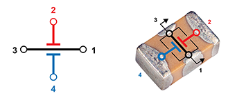

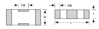
| 0402 (EMCF) |
0603 (EMCP) |
0805 (EMCT) |
1206 (EMDD) |
1210 (EMFD) |
1410 (EMDK) |
1812 (EMDR) |
||||||||
|---|---|---|---|---|---|---|---|---|---|---|---|---|---|---|
| IN | mm | IN | mm | IN | mm | IN | mm | IN | mm | IN | mm | IN | mm | |
| L | 0.045 ± 0.003 |
1.143 ± 0.076 |
0.064 ± 0.005 |
1.626 ± 0.127 |
0.080 ± 0.008 |
2.032 ± 0.203 |
0.124 ± 0.010 |
3.150 ± 0.254 |
0.125 ± 0.010 |
3.175 ± 0.254 |
0.140 ± 0.010 |
3.556 ± 0.254 |
0.174 ± 0.010 |
4.420 ± 0.254 |
| W | 0.025 ± 0.003 |
0.635 ± 0.076 |
0.035 ± 0.005 |
0.889 ± 0.127 |
0.050 ± 0.008 |
1.270 ± 0.203 |
0.063 ± 0.010 |
1.600 ± 0.254 |
0.098 ± 0.010 |
2.489 ± 0.254 |
0.098 ± 0.010 |
2.490 ± 0.254 |
0.125 ± 0.010 |
3.175 ± 0.254 |
| T | 0.02 max. |
0.508 max. |
0.26 max. |
0.660 max. |
0.040 max. |
1.016 max. |
0.050 max. |
1.270 max. |
0.070 max. |
1.778 max. |
0.070 max. |
1.778 max. |
0.090 max. |
2.286 max. |
| EB | 0.008 ± 0.003 |
0.203 ± 0.076 |
0.010 ± 0.006 |
0.254 ± 0.152 |
0.012 ± 0.008 |
0.305 ± 0.203 |
0.016 ± 0.010 |
0.406 ± 0.254 |
0.018 ± 0.010 |
0.457 ± 0.254 |
0.018 ± 0.010 |
0.457 ± 0.254 |
0.022 ± 0.012 |
0.559 ± 0.305 |
| CB | 0.012 ± 0.003 |
0.305 ± 0.076 |
0.018 ± 0.004 |
0.457 ± 0.102 |
0.022 ± 0.005 |
0.559 ± 0.127 |
0.040 ± 0.005 |
1.016 ± 0.127 |
0.045 ± 0.005 |
1.143 ± 0.127 |
0.045 ± 0.005 |
1.143 ± 0.127 |
0.045 ± 0.005 |
1.143 ± 0.127 |
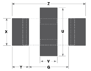
EMI Component & Pad Sizes
| Physical Dimensions |
0402 (EMCF) | 0603 (EMCP) | 0805 (EMCT) | 1206 (EMDD) | 1210 (EMFD) | 1410 (EMDK) | 1812 (EMDR) | ||||||||
|---|---|---|---|---|---|---|---|---|---|---|---|---|---|---|---|
| IN | mm | IN | mm | IN | mm | IN | mm | IN | mm | IN | mm | IN | mm | ||
| Chip | L | 0.045 ±.003 |
1.143 ±.076 |
0.064 ±.005 |
1.626 ±.127 |
0.080 ±.008 |
2.032 ±.203 |
0.124 ±.010 |
3.150 ±.254 |
0.125 ±.010 |
3.175 ±.010 |
0.140 ±.010 |
3.556 ±.254 |
0.174 ±.010 |
4.420 ±.254 |
| W | 0.025 ±.003 |
0.635 ±.076 |
0.035 ±.005 |
0.889 ±.127 |
0.050 ±.008 |
1.270 ±.203 |
0.063 ±.010 |
1.600 ±.254 |
0.098 ±.010 |
2.489 ±.254 |
0.098 ±.010 |
2.490 ±.254 |
0.125 ±.010 |
3.175 ±.254 |
|
| T | 0.020 max. |
0.508 max. |
0.026 max. |
0.660 max. |
0.040 max. |
1.016 max. |
0.050 max. |
1.270 max. |
0.070 max. |
1.778 max. |
0.070 max. |
1.778 max. |
0.090 max. |
2.286 max. |
|
| EB | 0.008 ±.003 |
0.203 ±.076 |
0.010 ±.006 |
0.254 ±.152 |
0.012 ±.008 |
0.305 ±.203 |
0.016 ±.010 |
0.406 ±.254 |
0.018 ±.010 |
0.457 ±.254 |
0.018 ±.010 |
0.457 ±.254 |
0.022 ±.012 |
0.559 ±.305 |
|
| CB | 0.012 ±.003 |
0.305 ±.076 |
0.018 ±.004 |
0.457 ±.102 |
0.022 ±.005 |
0.559 ±.127 |
0.040 ±.005 |
1.016 ±.127 |
0.045 ±.005 |
1.143 ±.127 |
0.045 ±.005 |
1.143 ±.127 |
0.045 ±.005 |
1.143 ±.127 |
|
| Solder Pad | X | 0.020 | 0.51 | 0.035 | 0.89 | 0.050 | 1.27 | 0.065 | 1.65 | 0.100 | 2.54 | 0.100 | 2.54 | 0.125 | 3.18 |
| Y | 0.018 | 0.45 | 0.025 | 0.64 | 0.035 | 0.89 | 0.040 | 1.02 | 0.040 | 1.02 | 0.040 | 1.02 | 0.040 | 1.02 | |
| G | 0.028 | 0.71 | 0.040 | 1.02 | 0.050 | 1.27 | 0.080 | 2.03 | 0.080 | 2.03 | 0.100 | 2.54 | 0.130 | 3.30 | |
| V | 0.013 | 0.33 | 0.020 | 0.51 | 0.022 | 0.56 | 0.040 | 1.02 | 0.045 | 1.14 | 0.045 | 1.14 | 0.045 | 1.14 | |
| U | 0.039 | 0.99 | 0.060 | 1.52 | 0.080 | 2.03 | 0.120 | 3.05 | 0.160 | 4.06 | 0.160 | 4.06 | 0.190 | 4.83 | |
| Z | 0.064 | 1.63 | 0.090 | 2.29 | 0.120 | 3.05 | 0.160 | 4.06 | 0.160 | 4.06 | 0.180 | 4.57 | 0.210 | 5.33 | |
|
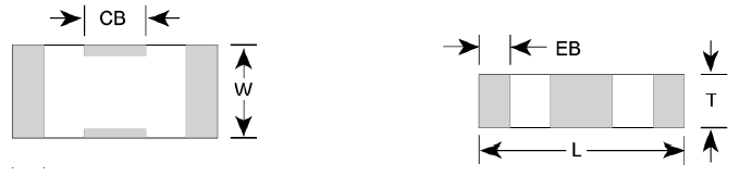
Solder mask beneath component should be avoided or minimized to reduce flux & containment entrapment |
||||||||||||||
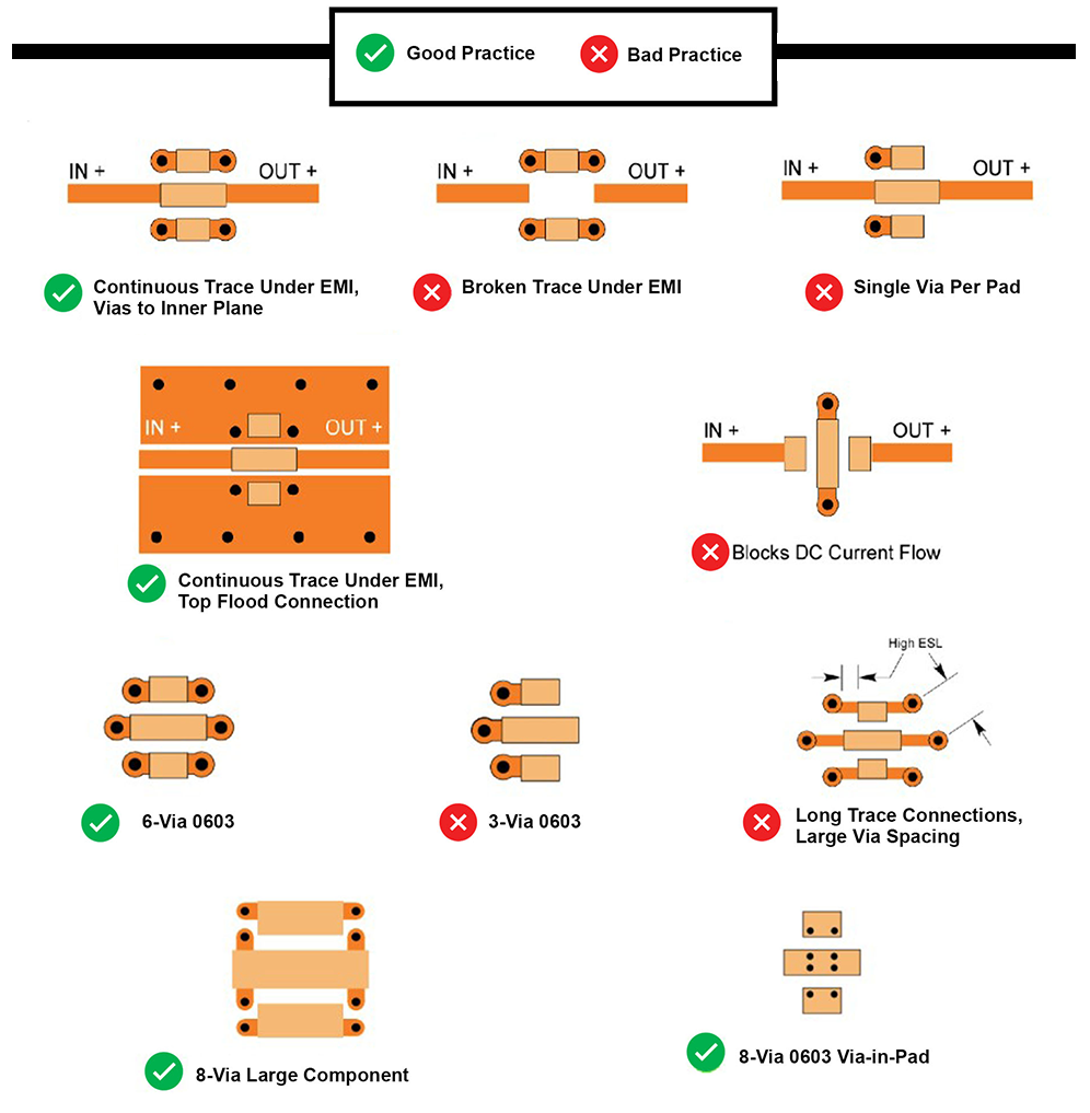
Trace - Via Layout Summary
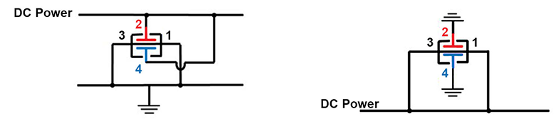
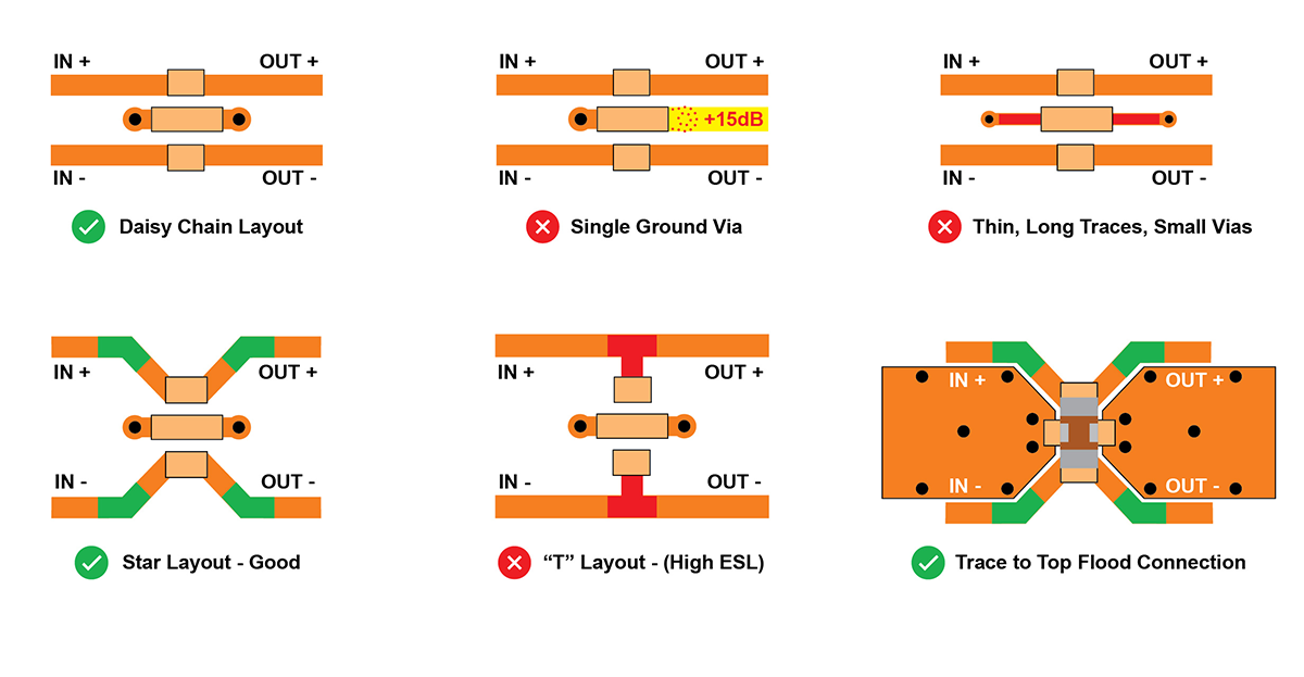
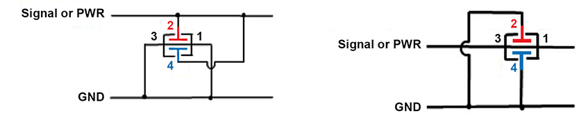
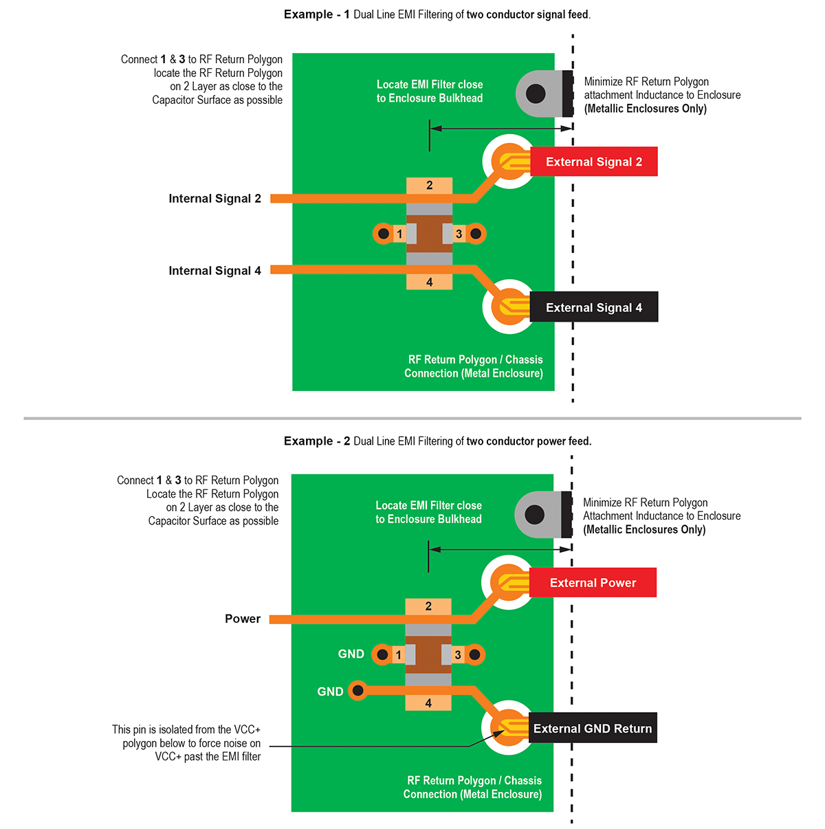
The following are key elements of Good Mounting Practice when applying EMI components with traces and vias on the PCB.
Differential Configuration - Trace & Via Layouts
Single-Ended Configuration - Trace & Via Layouts
Dual-Line EMI Filtering - Examples 1 & 2
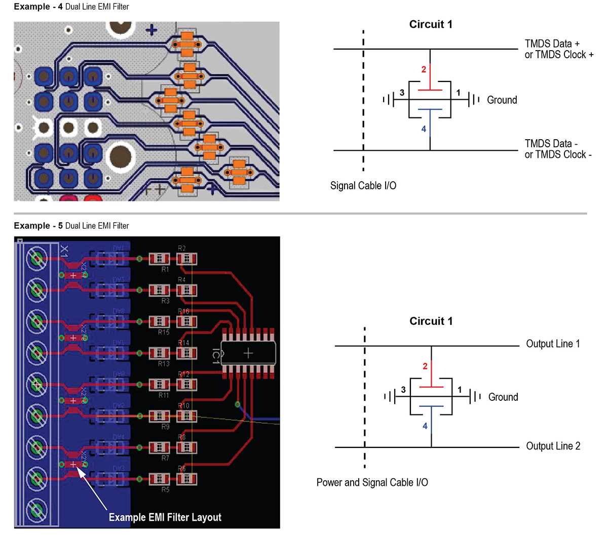
Dual Line EMI Filtering - Examples 4 & 5
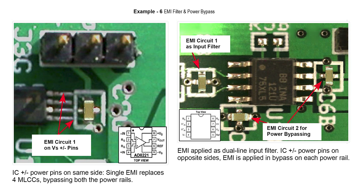
EMI Filter & Power Bypass - Example 6
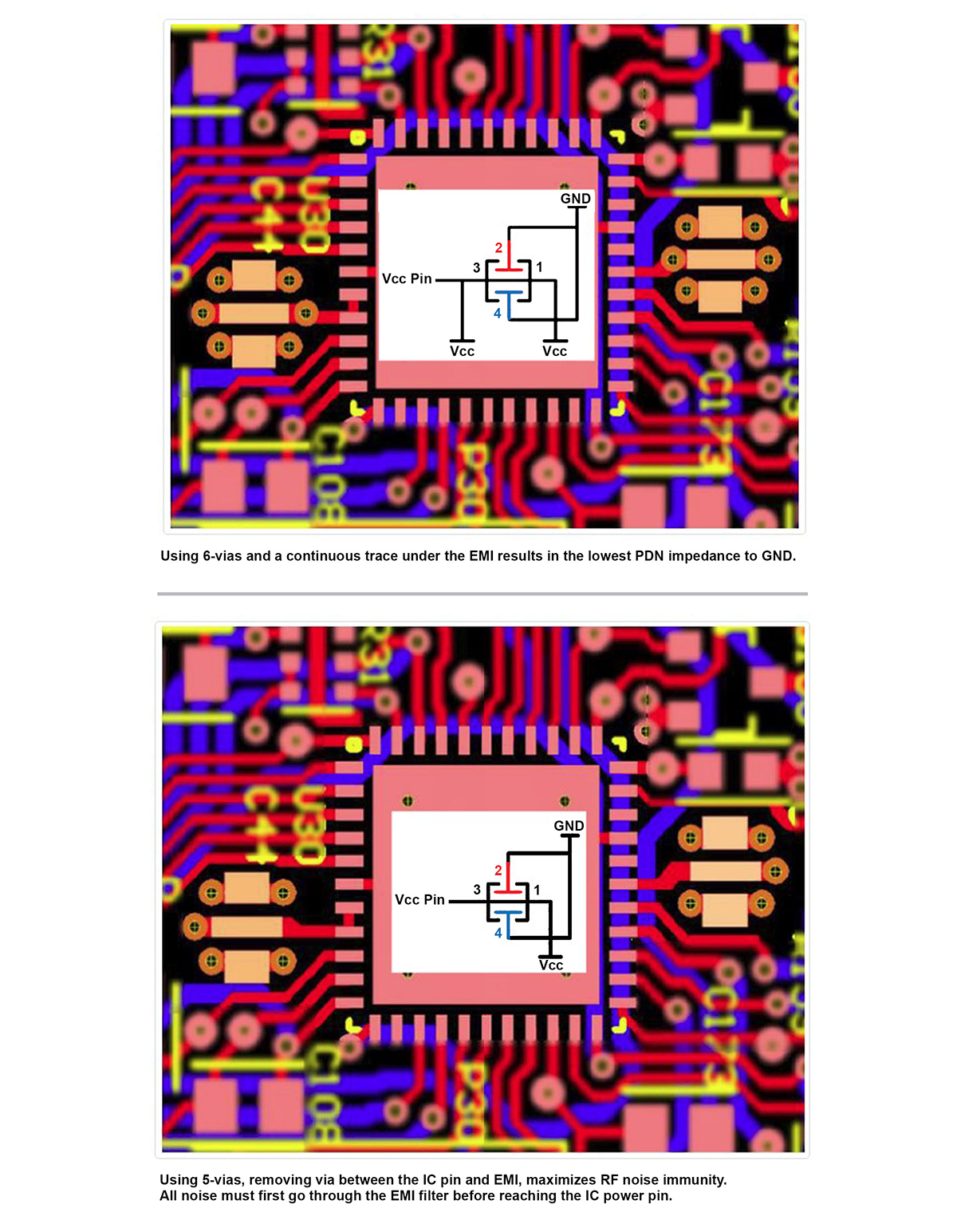
IC Power Bypass: Inner Planes Attachment
Multiple EMI components are attached between the inner Vcc an GND planes on this PCB for FPGA power bypassing.
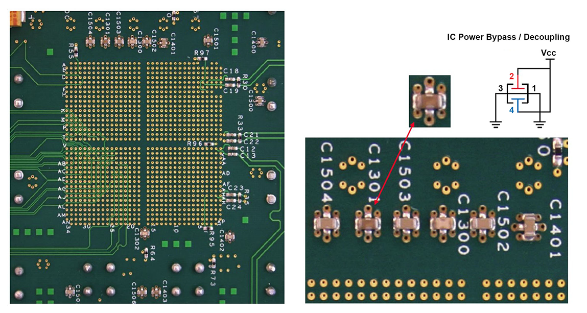
IC Power Bypass: Inner Planes Attachment
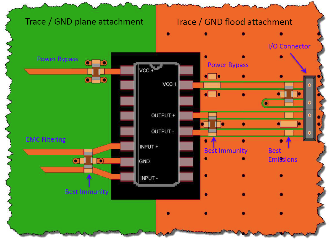
IC Power Bypass: Reduced EMC
We're here to help
Johanson provides first time adopters with application engineering assistance including part selection, schematic design review and PCB layout review.
Contact your Johanson Applications Engineer for more information by clicking here: Ask a Question
Thank You for your interest in our EMI Solutions