Multi-Layer Low ESR High-Q Capacitors
L-Series C-Series S-Series E-Series
These lines of Multi-Layer High-Q Capacitors, HiQ MLCC, HiQ Capacitors, SMT Capacitors, Low ESR Capacitors and Low Loss Capacitors have been developed for High-Q and microwave applications.
L-Series
Low Power
EIA 0201 (R05L) NPO/COGExample P/N: 250R05L100JV4T
These capacitors give mid-high Q performance, and exhibit NP0 temperature characteristics.
C-Series

Medium Power
EIA 0402 (QCCF) NPO/COGExample P/N: QCCF251Q0R7B1GV001T
EIA 0603 (QCCP) NPO/COGExample P/N: QCCP501Q100J1GV001T
EIA 0805 (QCCT) NPO/COGExample P/N: QCCT501Q121JGV001T
Ultra-high Q and low ESR performance with NPO characteristics.
S-Series

Medium Power
EIA 0402 (R07S) NPO/COGExample P/N:
201R07S4R7BV4T
Example P/N:
251R14S101JV4T
Example P/N:
251R15S470JV4E
Ultra-high Q and low ESR performance with NPO characteristics.
E-Series

High Power
EIA 1111 (S42E) NPO/COGExample P/N:
102S42E391GV3E
Example P/N:
252S48E360GU3W
Example P/N:
362S58E101JU3W
Excellent high-Q, low ESR and high RF power, from HF to microwave.
Multi-Layer/Low ESR High-Q Capacitors Information
Voltage Ratings
| EIA Size/Cap. Value | Miniature Size - Portable Electronics | RF Power Applications | ||||||||||||||||
|---|---|---|---|---|---|---|---|---|---|---|---|---|---|---|---|---|---|---|
| 0201 (R05) | NEW | NEW | NEW | |||||||||||||||
| NPO (R05L) | 0402 (R07S) | 0402 (QCCF) | 0603 (R14S) | 0603 (QCCP) | 0805 (R15S) | 0805 (R15L) | 0805 (QCCT) | 1111 (S42E) | 2525 (S48E) | 3838 (S58E) | ||||||||
| pF | Code | Voltage | ||||||||||||||||
| 0.1 | 0R1 | A B C D |
25/50V | 50/250V | 250V | 250V | 500V | 1000V | ||||||||||
| 0.2 | 0R2 | 25/50V | 50/250V | 250V | 250V | 500V | 1000V | 500V | 1500V | |||||||||
| 0.3 | 0R3 | 25/50V | 50/250V | 250V | 250V | 500V | 250V | 1000V | 500V | 1500V | ||||||||
| 0.4 | 0R4 | 25/50V | 50/250V | 250V | 250V | 500V | 250V | 1000V | 500V | 1500V | ||||||||
| 0.5 | 0R5 | 25/50V | 50/250V | 250V | 250V | 500V | 250V | 1000V | 500V | 1500V | 3600V | |||||||
| 0.6 | 0R6 | 25/50V | 50/250V | 250V | 250V | 500V | 250V | 1000V | 500V | 1500V | 3600V | 3600V | 7200V | |||||
| 0.7 | 0R7 | 25/50V | 50/250V | 250V | 250V | 500V | 250V | 1000V | 500V | 1500V | 3600V | 3600V | 7200V | |||||
| 0.8 | 0R8 | 25/50V | 50/250V | 250V | 250V | 500V | 250V | 1000V | 500V | 1500V | 3600V | 3600V | 7200V | |||||
| 0.9 | 0R9 | 25/50V | 50/250V | 250V | 250V | 500V | 250V | 1000V | 500V | 1500V | 3600V | 3600V | 7200V | |||||
| 1.0 | 1R0 | 25/50V | 50/250V | 250V | 250V | 500V | 250V | 1000V | 500V | 1500V | 3600V | 3600V | 7200V | |||||
| 1.1 | 1R1 | 25/50V | 50/250V | 250V | 250V | 500V | 250V | 1000V | 500V | 1500V | 3600V | 3600V | 7200V | |||||
| 1.2 | 1R2 | 25/50V | 50/250V | 250V | 250V | 500V | 250V | 1000V | 500V | 1500V | 3600V | 3600V | 7200V | |||||
| 1.3 | 1R3 | 25/50V | 50/250V | 250V | 250V | 500V | 250V | 1000V | 500V | 1500V | 3600V | 3600V | 7200V | |||||
| 1.4 | 1R4 | 25/50V | 50/250V | 250V | 250V | 500V | 250V | 1000V | 500V | 1500V | 3600V | 3600V | 7200V | |||||
| 1.5 | 1R5 | 25/50V | 50/250V | 250V | 250V | 500V | 250V | 1000V | 500V | 1500V | 3600V | 3600V | 7200V | |||||
| 1.6 | 1R6 | 25/50V | 50/250V | 250V | 250V | 500V | 250V | 1000V | 500V | 1500V | 3600V | 3600V | 7200V | |||||
| 1.7 | 1R7 | 25/50V | 50/250V | 250V | 250V | 500V | 250V | 1000V | 500V | 1500V | 3600V | 3600V | 7200V | |||||
| 1.8 | 1R8 | 25/50V | 50/250V | 250V | 250V | 500V | 250V | 1000V | 500V | 1500V | 3600V | 3600V | 7200V | |||||
| 1.9 | 1R9 | 25/50V | 50/250V | 250V | 250V | 500V | 250V | 1000V | 500V | 1500V | 3600V | 3600V | 7200V | |||||
| 2.0 | 2R0 | 25/50V | 50/250V | 250V | 250V | 500V | 250V | 1000V | 500V | 1500V | 3600V | 3600V | 7200V | |||||
| 2.1 | 2R1 | 25/50V | 50/250V | 250V | 250V | 500V | 250V | 1000V | 500V | 1500V | 3600V | 3600V | 7200V | |||||
| 2.2 | 2R2 | 25/50V | 50/250V | 250V | 250V | 500V | 250V | 1000V | 500V | 1500V | 3600V | 3600V | 7200V | |||||
| 2.4 | 2R4 | 25/50V | 50/250V | 250V | 250V | 500V | 250V | 1000V | 500V | 1500V | 3600V | 3600V | 7200V | |||||
| 2.7 | 2R7 | 25/50V | 50/250V | 250V | 250V | 500V | 250V | 1000V | 500V | 1500V | 3600V | 3600V | 7200V | |||||
| 3.0 | 3R0 | 25/50V | 50/250V | 250V | 250V | 500V | 250V | 1000V | 500V | 1500V | 3600V | 3600V | 7200V | |||||
| 3.3 | 3R3 | 25/50V | 50/250V | 250V | 250V | 500V | 250V | 1000V | 500V | 1500V | 3600V | 3600V | 7200V | |||||
| 3.6 | 3R6 | 25/50V | 50/200V | 250V | 250V | 500V | 250V | 1000V | 500V | 1500V | 3600V | 3600V | 7200V | |||||
| 3.9 | 3R9 | 25/50V | 50/200V | 250V | 250V | 500V | 250V | 1000V | 500V | 1500V | 3600V | 3600V | 7200V | |||||
| 4.3 | 4R3 | 25/50V | 50/200V | 250V | 250V | 500V | 250V | 1000V | 500V | 1500V | 3600V | 3600V | 7200V | |||||
| 4.7 | 4R7 | 25/50V | 50/200V | 250V | 250V | 500V | 250V | 1000V | 500V | 1500V | 3600V | 3600V | 7200V | |||||
| 5.1 | 5R1 | B C D |
25/50V | 50/200V | 250V | 250V | 500V | 250V | 1000V | 500V | 1500V | 3600V | 3600V | 7200V | ||||
| 5.6 | 5R6 | 25/50V | 50/200V | 250V | 250V | 500V | 250V | 1000V | 500V | 1500V | 3600V | 3600V | 7200V | |||||
| 6.2 | 6R2 | 25/50V | 50/200V | 250V | 250V | 500V | 250V | 1000V | 500V | 1500V | 3600V | 3600V | 7200V | |||||
| 6.8 | 6R8 | 25/50V | 50/200V | 250V | 250V | 500V | 250V | 1000V | 500V | 1500V | 3600V | 3600V | 7200V | |||||
| 7.5 | 7R5 | 25/50V | 50/200V | 250V | 250V | 500V | 250V | 1000V | 500V | 1500V | 3600V | 3600V | 7200V | |||||
| 8.2 | 8R2 | 25/50V | 50/200V | 250V | 250V | 500V | 250V | 1000V | 500V | 1500V | 3600V | 3600V | 7200V | |||||
| 9.1 | 9R1 | 25/50V | 50/200V | 250V | 250V | 500V | 250V | 1000V | 500V | 1500V | 3600V | 3600V | 7200V | |||||
| 10 | 100 | F G J K |
25/50V | 50/200V | 250V | 250V | 500V | 250V | 1000V | 500V | 1500V | 3600V | 3600V | 7200V | ||||
| 11 | 110 | 25/50V | 50/200V | 250V | 250V | 500V | 250V | 1000V | 500V | 1500V | 3600V | 3600V | 7200V | |||||
| 12 | 120 | 25/50V | 50/200V | 250V | 250V | 500V | 250V | 1000V | 500V | 1500V | 3600V | 3600V | 7200V | |||||
| 13 | 130 | 25/50V | 50/200V | 250V | 250V | 500V | 250V | 1000V | 500V | 1500V | 3600V | 3600V | 7200V | |||||
| 15 | 150 | 25/50V | 50/200V | 250V | 250V | 500V | 250V | 1000V | 500V | 1500V | 3600V | 3600V | 7200V | |||||
| 16 | 160 | 25/50V | 50/200V | 250V | 250V | 500V | 250V | 1000V | 500V | 1500V | 3600V | 3600V | 7200V | |||||
| 18 | 180 | 25/50V | 50/200V | 250V | 250V | 500V | 250V | 1000V | 500V | 1500V | 3600V | 3600V | 7200V | |||||
| 20 | 200 | 25/50V | 50/200V | 250V | 250V | 500V | 250V | 1000V | 500V | 1500V | 3600V | 3600V | 7200V | |||||
| 22 | 220 | 25/50V | 50/200V | 250V | 250V | 500V | 250V | 1000V | 500V | 1500V | 3600V | 3600V | 7200V | |||||
| 24 | 240 | 25/50V | 50/200V | 250V | 250V | 500V | 250V | 1000V | 500V | 1500V | 3600V | 3600V | 7200V | |||||
| 27 | 270 | 25/50V | 50/200V | 250V | 250V | 500V | 250V | 1000V | 500V | 1500V | 3600V | 3600V | 7200V | |||||
| 30 | 300 | 25/50V | 50V | 250V | 250V | 500V | 250V | 1000V | 500V | 1500V | 3600V | 3600V | 7200V | |||||
| 33 | 330 | 25/50V | 50V | 250V | 250V | 500V | 250V | 1000V | 500V | 1500V | 3600V | 3600V | 7200V | |||||
| 36 | 360 | F G J K |
25/50V | 250V | 500V | 250V | 1000V | 500V | 1500V | 3600V | 3600V | 7200V | ||||||
| 39 | 390 | 25/50V | 250V | 500V | 250V | 1000V | 500V | 1500V | 3600V | 3600V | 7200V | |||||||
| 43 | 430 | 25/50V | 250V | 500V | 250V | 1000V | 500V | 1500V | 3600V | 3600V | 7200V | |||||||
| 47 | 470 | 25/50V | 250V | 500V | 250V | 1000V | 500V | 1500V | 3600V | 3600V | 7200V | |||||||
| 51 | 510 | 25/50V | 250V | 500V | 250V | 1000V | 500V | 1500V | 3600V | 3600V | 7200V | |||||||
| 56 | 560 | 25/50V | 250V | 500V | 250V | 1000V | 500V | 1500V | 3600V | 3600V | 7200V | |||||||
| 62 | 620 | 25/50V | 250V | 500V | 250V | 1000V | 500V | 1500V | 3600V | 3600V | 7200V | |||||||
| 68 | 680 | 25/50V | 250V | 500V | 250V | 1000V | 500V | 1500V | 3600V | 3600V | 7200V | |||||||
| 75 | 750 | 25/50V | 250V | 500V | 250V | 1000V | 500V | 1500V | 3600V | 3600V | 7200V | |||||||
| 82 | 820 | 25/50V | 250V | 500V | 250V | 1000V | 500V | 1500V | 3600V | 3600V | 7200V | |||||||
| 91 | 910 | 25/50V | 250V | 500V | 250V | 1000V | 500V | 1500V | 3600V | 3600V | 7200V | |||||||
| 100 | 101 | 25/50V | 250V | 500V | 250V | 1000V | 500V | 1500V | 3600V | 3600V | 7200V | |||||||
| 110 | 111 | 250V | 500V | 300V | 1500V | 2500V | 3600V | 7200V | ||||||||||
| 120 | 121 | 250V | 500V | 300V | 1000V | 2500V | 3600V | 7200V | ||||||||||
| 130 | 131 | 250V | 500V | 300V | 1000V | 2500V | 3600V | 7200V | ||||||||||
| 150 | 151 | 250V | 500V | 300V | 1000V | 2500V | 3600V | 7200V | ||||||||||
| 160 | 161 | 250V | 500V | 300V | 1000V | 2500V | 3600V | 7200V | ||||||||||
| 180 | 181 | 250V | 500V | 300V | 1000V | 2500V | 3600V | 7200V | ||||||||||
| 200 | 201 | 250V | 500V | 300V | 1000V | 2500V | 3600V | |||||||||||
| 220 | 221 | 250V | 500V | 200V | 1000V | 2500V | 3600V | |||||||||||
| 240 | 241 | 200/500V | 200V | 600V | 2500V | 3600V | ||||||||||||
| 270 | 271 | 200/500V | 200V | 600V | 2500V | 3600V | ||||||||||||
| 300 | 301 | 200/500V | 200V | 600V | 1500V | 3600V | ||||||||||||
| 330 | 331 | 200/500V | 200V | 600V | 1500V | 3600V | ||||||||||||
| 360 | 361 | 200/500V | 200V | 600V | 1500V | 3600V | ||||||||||||
| 390 | 391 | 200/500V | 200V | 500V | 1500V | 3600V | ||||||||||||
| 430 | 431 | F G J K |
200/500V | 200V | 500V | 1500V | 2500V | |||||||||||
| 470 | 471 | 500V | 200V | 500V | 1500V | 2500V | ||||||||||||
| 510 | 511 | 100V | 200V | 500V | 1000V | 2500V | ||||||||||||
| 560 | 561 | 100V | 200V | 500V | 1000V | 2500V | ||||||||||||
| 620 | 621 | 100V | 200V | 500V | 1000V | 2500V | ||||||||||||
| 680 | 681 | 50V | 200V | 1000V | 2500V | |||||||||||||
| 750 | 751 | 50V | 200V | 1000V | 2500V | |||||||||||||
| 820 | 821 | 50V | 200V | 1000V | 2500V | |||||||||||||
| 910 | 911 | 50V | 200V | 1000V | 1000V | |||||||||||||
| 1000 | 102 | 50V | 200V | 1000V | 1000V | |||||||||||||
| 1200 | 122 | 50V | 1000V | 1000V | ||||||||||||||
| 1500 | 152 | 50V | 500V | 1000V | ||||||||||||||
| 1800 | 182 | 50V | 500V | 1000V | ||||||||||||||
| 2200 | 222 | 50V | 300V | 1000V | ||||||||||||||
| 2700 | 272 | 300V | 500V | |||||||||||||||
| 3300 | 332 | 500V | ||||||||||||||||
| 3900 | 392 | 500V | ||||||||||||||||
| 4700 | 472 | 500V | ||||||||||||||||
| 5100 | 512 | 500V | ||||||||||||||||
| 10000 | 103 | |||||||||||||||||
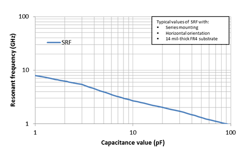
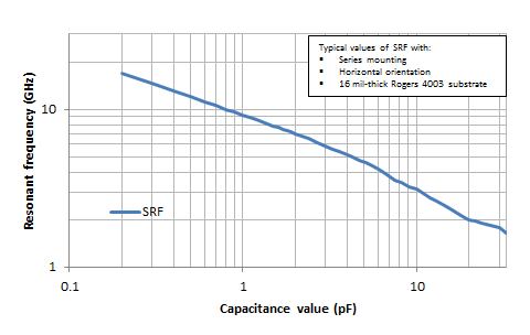
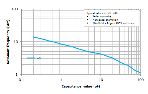
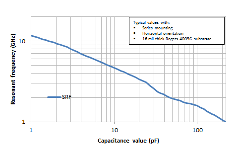
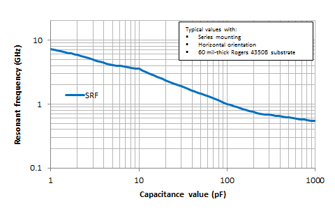
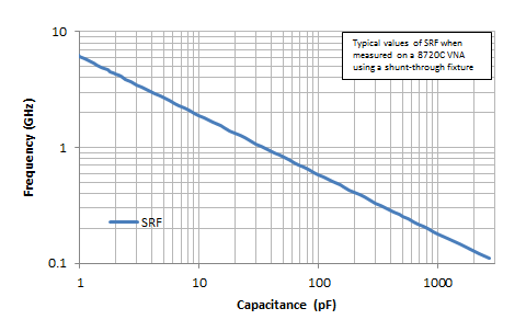
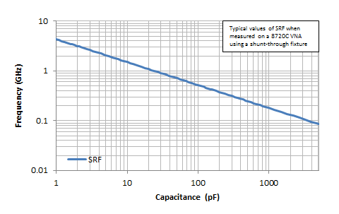
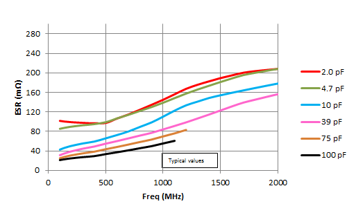
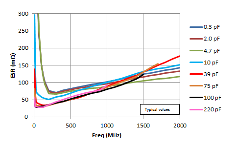
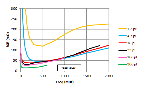
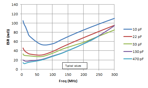
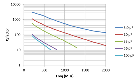
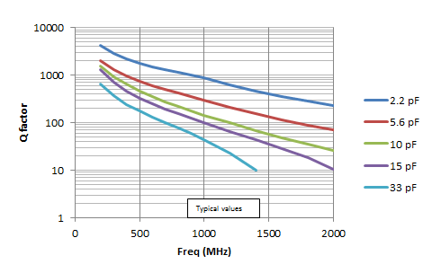
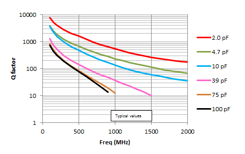
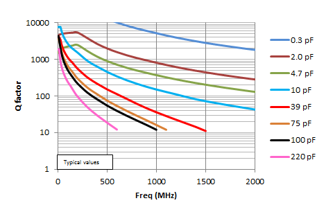
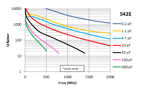
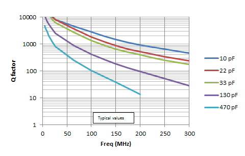
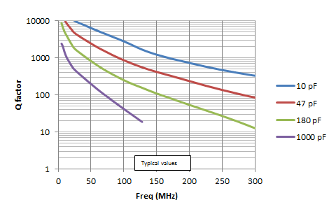
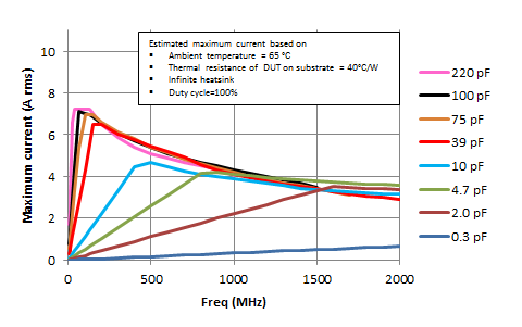
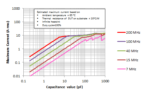
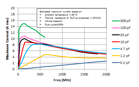
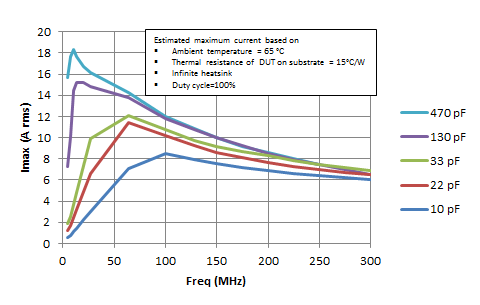
Resonant frequencies
The Series Resonant Frequency is highly dependent on the substrate, pad dimensions, and measurement method. The below charts are for reference only.
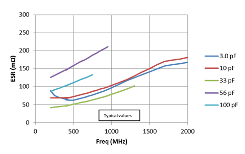
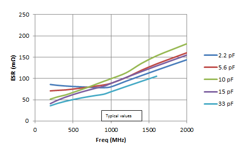
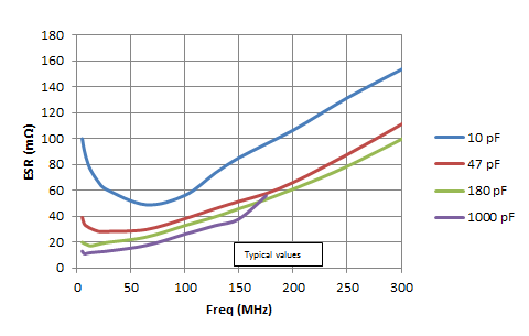
ESR curves
Q factor curves
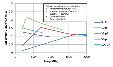
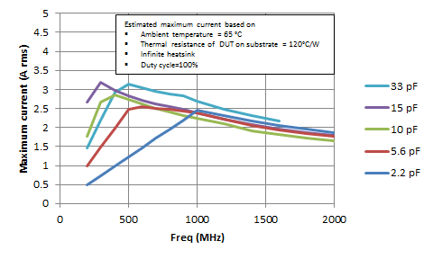
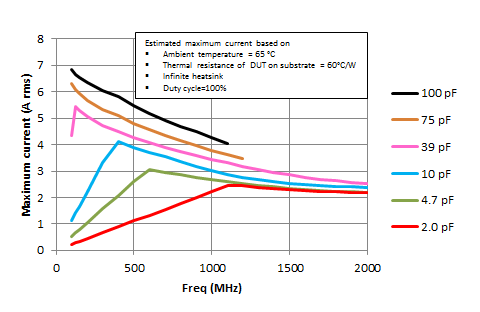
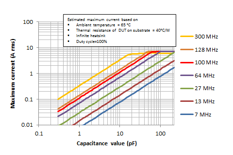
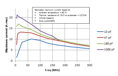
Max RF current
Dielectric Characteristics
| NPO | |
| Temperature Coefficient: | 0 ± 30ppm /°C, -55 to 150°C |
|---|---|
| Quality Factor / DF: | Q >1,000 @ 1 MHz, Typical 10,000 |
| Insulation Resistance: | >10 GΩ @ 25°C,WVDC; 125°C IR is 10% of 25°C rating |
| Dielectric Strength: | 2.5 X WVDC Min., 25°C, 50 mA max |
| Test Parameters: | 1MHz ±50kHz, 1.0±0.2VRMS for capacitance values ≤ 1,000pF 1kHZ ±50Hz, 1.0±0.2VRMS for capacitance values > 1,000pF |
| Available Capacitance: | Size 0201: 0.2 - 100 pF Size 0402: 0.2 - 33 pF Size 0603: 0.2 - 100 pF Size 0805: 0.3 - 220 pF Size 1111: 0.2 - 1000 pF Size 2525: 0.5 - 2700 pF Size 3838: 0.5 - 5100 pF |
Mechanical Characteristics
| Size | Units | Length | Width | Thickness | End Band |
|---|---|---|---|---|---|
| EIA 0201 | In | .024 ± .001 | .012 ± .001 | .012 ± .001 | .008 Max. |
| Metric (0603) | mm | (0.60 ± 0.03) | (0.30 ± 0.03) | (0.30 ± 0.03) | (0.20 Max.) |
| EIA 0402 | In | .040 ± .004 | .020 ± .004 | .020 ± .004 | .010 ± .006 |
| Metric (1005) | mm | (1.02 ± 0.1) | (0.51 ± 0.1) | (0.51 ± 0.1) | (0.25 ± .15) |
| EIA 0603 | In | .062 ± .006 | .032 ± .006 | .030 + .005 /- .003 | .014 ± .006 |
| Metric (1608) | mm | (1.57 ± 0.15) | (0.81 ± 0.15) | (0.76 + .13 - .08) | (0.35 ± .15) |
| EIA 0805 | In | .080 ± .008 | .050 ± .008 | .040 ± .006 | .020 ± .010 |
| Metric (2012) | mm | (2.03 ± 0.20) | (1.27 ± 0.20) | (1.02 ± .15) | (0.50 ± .25) |
Environmental Characteristics
| Specification | Test Parameters | |
|---|---|---|
| Solderability: | Solder coverage ≥ 90% of metalized areas No termination degradation | Preheat chip to 120°-150°C for 60 sec., dip terminals in rosin flux then dip in Sn62 solder @ 240°±5°C for 5±1 sec |
| Resistance to Soldering Heat : | No mechanical damage Capacitance change: ±2.5% or 0.25pF Q>500 I.R. >10 G Ohms Breakdown voltage: 2.5 x WVDC |
Preheat device to 80°-100°C for 60 sec. followed by 150°-180°C for 60 sec. Dip in 260°±5°C solder for 10±1 sec. Measure after 24±2 hour cooling period |
| Terminal Adhesion: | Termination should not pull off. Ceramic should remain undamaged. |
Linear pull force* exerted on axial leads soldered to each terminal. *0402 ≥ 2.0lbs, 0603 ≥ 4.0lbs (min.) |
| PCB Deflection: | No mechanical damage. Capacitance change: 2% or 0.5pF Max |
Glass epoxy PCB: 0.5 mm deflection |
| Vibration: | No mechanical damage. Capacitance change: ±2.5% or 0.25pF Q>1000 I.R. ≥ 10 G-Ohm Breakdown voltage: 2.5 x WVDC |
Cycle performed for 2 hours in each of three perpendicular directions. Frequency range 10Hz to 55 Hz to 10 Hz traversed in 1 minute. Harmonic motion amplitude: 1.5mm. |
| Humidity, Steady State: | No mechanical damage. Capacitance change: ±5.0% or 0.50pF max. Q>300 I.R. ≥ 1 G-Ohm Breakdown voltage: 2.5 x WVDC |
Relative humidity: 90-95% Temperature: 40°±2°C Test time: 500 +12/-0 Hours Measure after 24±2 hour cooling period |
| Humidity, Low Voltage: | No mechanical damage. Capacitance change: ±5.0% or 0.50pF max. Q>300 I.R. = 1 G-Ohm min. Breakdown voltage: 2.5 x WVDC |
Applied voltage: 1.5 VDC, 50 mA max. Relative humidity: 85±2% Temperature: 40°±2°C Test time: 240 +12/-0 Hours Measure after 24±2 hour cooling period |
| Thermal Cycle: | No mechanical damage. Capacitance change: ±2.5% or 0.25pF Q>2000 I.R. >10 G Ohms Breakdown voltage: 2.5 x WVDC |
5 cycles of: 30±3 minutes @ -55°+0/-3°C, 2-3 min. @ 25°C, 30±3 min. @ +125°+3/-0°C, 2-3 min. @ 25°C Measure after 24±2 hour cooling period |
| Life Test: | MIL-STD-202, Method 1081 No mechanical damage. Capacitance change: ±3.0% or 0.3 pF Q>500 I.R. >1 G Ohms Breakdown voltage: 2.5 x WVDC |
Applied voltage: 200% of WDVC for capacitors rated at 500 volts DC or less. Temperature: 125°±3°C Test time: 1000+48-0 hours |
Automotive applications (AEC-Q200): additional requirements – please consult factory for details.
Chip Capacitor Tape & Reel Packaging
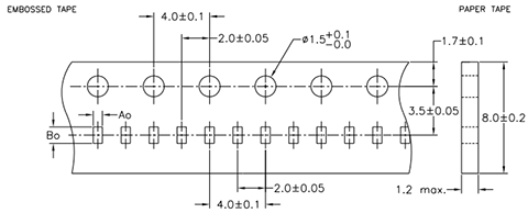
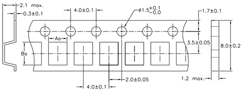
Johanson capacitors are available taped per EIA standard 481. Tape options include 5", 7" and 13" diameter reels. Johanson uses high quality, dust free, punched 8mm paper tape and plastic embossed 8mm tape for thicker MLCs. Quantity per reel ranges are listed in the tables below and are dependent on chip thickness.
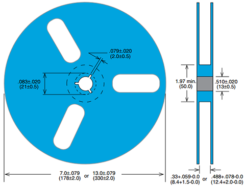
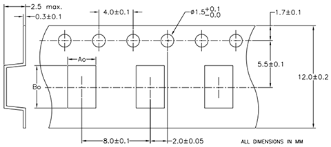
| 5” DIA. REEL SIZE | 7” DIA. REEL SIZE | 13” DIA. REEL SIZE | |||||||
|---|---|---|---|---|---|---|---|---|---|
| TYPE / SIZE | REEL QUANTITY | TAPE TYPE | TAPE CODE | REEL QUANTITY | TAPE TYPE | TAPE CODE | REEL QUANTITY | TAPE TYPE | TAPE CODE |
| R05 / 0201 | 500 | Paper | Y | 15,000 | Paper | T | N/A | N/A | N/A |
| R07 / 0402 | 500 | Paper | Y | 10,000 | Paper | T | N/A | N/A | N/A |
| R14 / 0603 | 500 | Paper | Y | 4,000 | Paper | T | 10,000 | Paper | R |
| R15 / 0805 | 500 | Embossed | Z | 4,000 | Embossed | E | 10,000 | Embossed | U |
| S42 / 1111 | 500 | Embossed | Z | 2,000 | Embossed | E | 10,000 | Embossed | U |
| S48 / 2525 | N/A | 250 | Embossed | E | 1,000 | Embossed | U | ||
| S58 / 3838 | N/A | 250 | Embossed | E | 1,000 | Embossed | U | ||
| LASERtrim® (All) | 500 | Paper | Y | 4.5-5.0K | Paper | T | 15,000 | Paper | R |
| SUBSTRATES – DEPENDS ON SIZE, TYPICAL IS 10/BOX CAP ARRAYS - 100/TRAY SINGLE LAYER CAPACITORS - UP TO 50 MIL, 400/WAFFLE PACK; > 50 MIL, 100/WAFFLE PACK SLC’S CAN ALSO BE MOUNTED ON GRIP RINGS, RING FRAMES, AND SURFTAPE CUSTOM PACKAGING AND QUANTITIES ARE AVAILABLE, CONTACT THE FACTORY FOR OPTIONS PLEASE VISIT OUR WEB SITE FOR RF CERAMIC COMPONENT PACKAGING INFORMATION. |
|||||||||
Soldering Profiles and Guidelines for SMT Ceramic Components
General
Ceramic chip capacitors exhibit excellent reliability characteristics providing that proper circuit design techniques and controlled assembly processes are utilized. Due to the ceramic capacitor’s crystalline micro-structure these components are susceptible when exposed to excessive thermal or mechanical shock during circuit processing. It should be noted that micro-cracks in ceramic can be difficult to detect with normal post assembly visual and electrical testing and can pose a significant threat to reliable field operation. For this reason it is recommended that the assembly qualification process employ suitable testing to expose the presence of micro-cracking conditions.
Ceramic components’ leads composition and soldering compatibility
High Frequency Ceramic Capacitors & Inductors - Offered with standard tin plated nickel-barrier terminations compatible with solder flow and reflow processes.
Single Layer Capacitors - Offered with Titanium-Tungsten/Gold and Titanium-Tungsten/ Nickel/Gold thin-film termination as well as legacy Platinum/Palladium/Gold terminations.
LASERtrim® Capacitors - Offered with gold flashed nickel-barrier terminations only. Due to the unique internal construction of the LASERtrim® it is recommended that a conservative reflow temperature profile be used (Fig. 5). Wave soldering is discouraged.
Soldering Iron
Ceramic capacitor attachment with a soldering iron is discouraged due to the inherent limitations on precisely controlling soldering temperature, heat transfer rate, and time. In the event that a soldering iron must be employed the following precautions are recommended.
- Preheat circuit and ceramic component to 150°C
- ever contact the ceramic surface with the iron tip
- 30 watt iron output (max)
- 280°C tip temperature (max)
- 3.0 mm tip diameter (max)
- Limit soldering time to 5 sec.
Solder Pre-Heat Cycle
Proper preheating is essential to prevent thermal shock cracking of the capacitor. The circuit assembly should be preheated as shown in the recommended profiles at a rate of 1.0 to 2.0°C per second to within 65 to 100°C of the maximum soldering temperature.
- Preheat circuit and ceramic component to 150°C
- ever contact the ceramic surface with the iron tip
- 30 watt iron output (max)
- 280°C tip temperature (max)
- 3.0 mm tip diameter (max)
- Limit soldering time to 5 sec.
SMT Soldering Temperatures
Solders typically utilized in SMT have melting points between 179°C and 188°C. Activation of rosin fluxes occurs at about 200°C. Based on these facts a minimum peak reflow temperature of 205°C to 210°C should be established. A maximum peak reflow temperature of 225°C should be adequate in most circumstances. Many reflow process profiles have peaks ranging from 240°C to 260°C and while ceramic capacitors and inductors can withstand soldering temperatures in this range for short durations they should be minimized or avoided whenever possible. Use of PCB mounted multiple thermocouple M.O.L.E. profiling is advised for accurate characterization of circuit heat absorption and maximum temperature conditions.
Reflow Solder
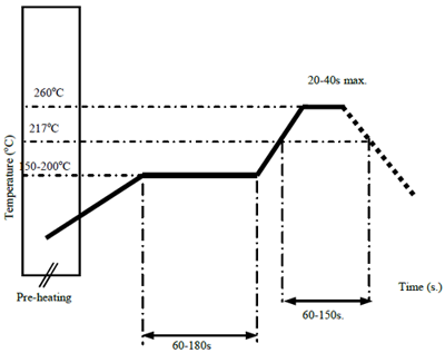
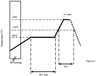
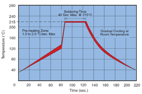
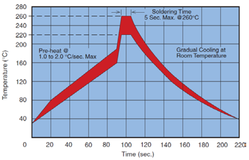
The general term “reflow” refers to several methods used in heating the circuit so that solder paste reflows, or “wetting” of the ceramic capacitor and PCB contacts occurs. These methods include infrared, convection and radiant heating. The size of the solder fillet may be controlled by varying the amount of solder paste that is screened onto the circuit. Recommended temperature limits and times for solder reflow are shown in Figure 1 and 2 for Ceramic Capacitors and inductors and for LASERtrim® in Figure 5.
Vapor Phase
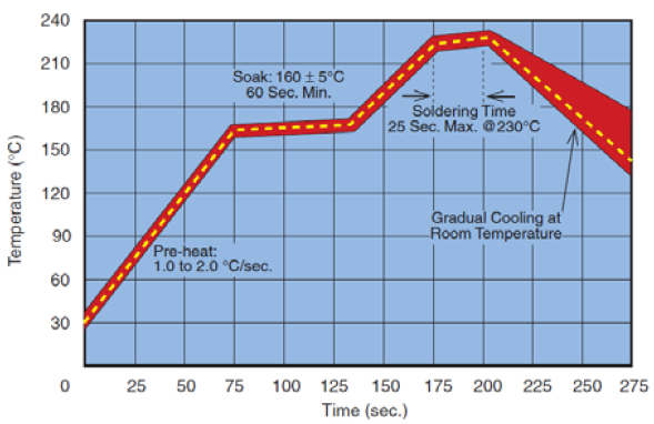
A typical vapor phase soldering process consists of several temperature zones created by saturated vapor from a boiling liquid. As the circuit passes through the zone the vapor condenses on the solder paste, pad, and termination resulting in heat transfer and reflow of the solder paste. Vapor phase reflow produces consistent circuit heating with reflow occurring at a relatively lower temperature that is determined by the known boiling point of the liquid used, typically 215°C. Recommended temperature limits for vapor phase reflow are shown in Figure 3.
Solder Wave
Wave soldering is perhaps the most rigorous of surface mount soldering processes due to the steep rise in temperature seen by the circuit as it is immersed in the molten solder wave, typically at 240°C. Recommended temperature limits for wave soldering are shown in Fig. 4.
Cool Down Cycle
After the solder reflows properly the assembly should be allowed to cool gradually at room ambient conditions. Attempts to speed this cooling process or immediate exposure of the circuit to cold cleaning solutions may result in thermal shock cracking of the ceramic capacitor.
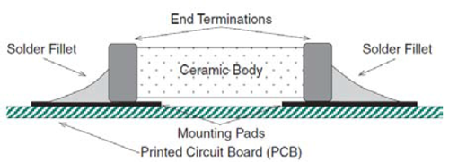
Solder Fillets
To avoid detrimental effects of thermal and mechanical stress it is essential that the solder fillet be limited to 2/3rds of the overall height of the MLC termination as illustrated in the figure below. The solder fillet can be controlled by solder paste deposition and pad design in reflow and vapor phase processes and by pad design and use of hot air knives in the wave process. As shown in Figure 6.
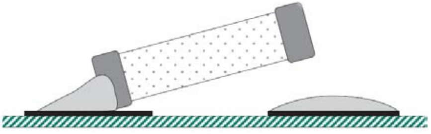
Tomb Stoning/Chip Movement
Tomb-stoning or draw bridging is illustrated in the figure below. Tomb-stoning or other undesirable chip movements may result if unequal surface tension forces exist as the molten solder wets the MLC terminations and mounting pads. This tendency can be minimized by insuring that all factors at both solder joints are equal, namely; pad size, solder mass, termination size, component position and heating. Tomb-stoning is easily avoided through proper design, material selection and proofing of the process. As shown in figure 7.
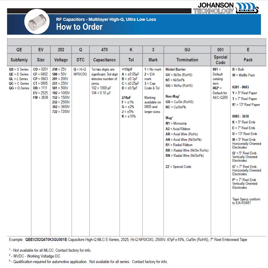
How to Order