Dishal Bandpass Filter Tuning Using LASERtrim® Chip Caps
Introductions:
A variation of the Dishal method of tuning bandpass filters by tuning isolated LC stages in succession is readily adaptable to a fully automated and highly accurate trimming process during manufacturing using Johanson Technology’s LASERtrim® surface mount tuning capacitors and zero ohm resistor jumpers which can be cut open during the laser trimming process. The same process can be used in compensation of component tolerances and stray capacitance as well as adjusting a single filter design for various frequency bandsplits.
Scope:
The design of filters is a vast topic and there are numerous textbooks on the subject. Thus design will not be covered in this application note. The information contained here is targeted for engineers and/or technicians who must tune the final filter circuit or design an algorithm for tuning. The procedure will be demonstrated by a series of figures showing the filter response of a 4-resonator VHF LC bandpass filter under various conditions. The filter response will be shown before and after tuning. In practice different filter designs will exhibit somewhat different responses. By using this approach, however, the proper response for each individual resonator of the particular design can be determined beforehand and then used in production to tune each resonator to the proper value.
Advantages:
Superior circuit performance may be achieved by optimizing the response of filters having relatively narrow bandwidths compared to the center frequency. For example consider a bandpass filter with a 100 MHz center frequency and 5 MHz bandwidth (i.e. Q=20). If 5% tolerance components are used, the center frequency could be skewed by +/- 5% in a worst case scenario (i.e. 5MHz). In this situation all of the frequencies that should fall into the pass band of the filter would actually end up in the stop band.
Another advantage in using a functionally tuned filter would be to reduce the parts count of the filter. Note that a common approach to avoid tuning is to over-design the filter by increasing the filter order such that stop band attenuation is guaranteed over tolerance. Also the passband must be widened to guarantee passband frequencies are not attenuated. Statistically the more parts there are in the filter the less chance there is of all of them being the worst case tolerance at the same time. Tuning out the component tolerance, however, allows one to use the minimum number of components necessary to get the desired response. For example consider the requirement for a Butterworth bandpass filter with a center frequency of 150 MHz, a 10 MHz wide 3 dB passband, and a stop band attenuation of 45 dB for frequencies below 130 MHz and above 170 MHz. This could be accomplished with a 4th order filter if the resonators are tuned. However, with 2% tolerance parts and no tuning an 8th order filter would be required to absorb the tolerance. Using 5% tolerance parts would be unacceptable because the stop band and passband edge would overlap (i.e. 155 MHz x 1.05 is greater then 170 MHz x 0.95).
A third advantage of tuned filters is that a common filter design can be utilized in RF circuits having multiple bandsplit filtering requirements. The alternative of using different sets of fixed value components for each bandsplit increases the part count and in many cases may be impractical due to the availability problems associated with non-standard value components.
Tuning Overview:
Dishal’s method of filter tuning is accomplished by selectively shorting to ground some of the resonators while the other resonators are being tuned. One by one the shorts across each resonator are removed and each resonator is tuned for the proper voltage response which is monitored at the first and last filter resonators. Rather than explaining the procedure further in general terms an example will be used to illustrate the procedure.
Tuning Example Part 1:
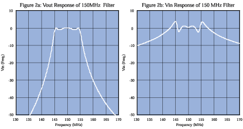
Consider the circuit in Figure 1a. It is comprised of four LC tanks coupled by capacitors. It is designed for 150 MHz center frequency, 10 MHz bandwidth, and a termination impedance of 1000 ohms. Figure 1b shows the filter circuit connected to a 1000 ohm source and load. Note that resistors have been placed in parallel with the 2nd, 3rd and 4th resonators. These resistors will be either short or open circuits during the tuning process.
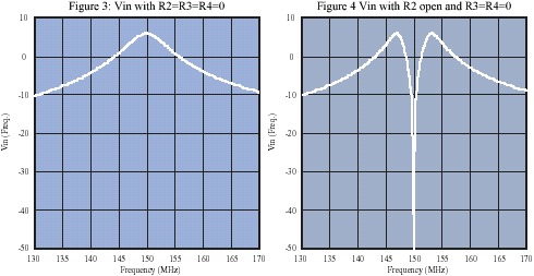
We will define the voltage at the first resonator as Vin and the voltage at the last resonator as Vout. The Vin and Vout frequency responses are shown in Figures 2a and 2b, respectively.
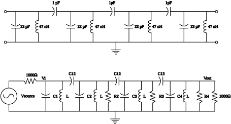
Figure 1a
The Vout response is equivalent to the filter bandpass response except it is not normalized to the Vsource voltage. For most of the tuning procedure Vin is the voltage of interest and is similar to monitoring a voltage input reflection coefficient. Note that the Vin response has three dips in the passband when the filter is centered. In this example the dip at 150 Mhz is not as deep as the other two.
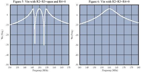
Now suppose we set R2, R3, and R4 equal to zero ohms. This leaves a resonant circuit consisting of L1, C1, and one C12 coupling capacitor. This will, of course, short out any signal that would normally appear at Vout. However, notice what happens to Vin. As is shown in Figure 3 the Vin response becomes a rounded passband-like response which is centered at 150 Mhz.
Now suppose we open circuit R2 while R3 and R4 are still short circuits. This adds L2, C2, and another coupling capacitor to the circuit. Figure 4 shows the effect on Vin. Rather than a peak at center frequency we now have a sharp null. In fact as we successively open circuit the resistors the Vin response will alternate between peaks and nulls at the center frequency. An odd number of resonators will result in peaks and an even number will result in nulls. Note that only the final LC resonator in the chain has a resistive load present. This affects the Vin response by making the nulls and peaks less pronounced. In our example if the 1k load were removed from the fourth resonator, the Vin response in Figure 2b would have three sharp nulls with the center null position at 150 MHz.
Now let’s open circuit R3 with R4 still shorted. This adds L3, C3, and a coupling capacitor to our previous circuit. Figure 5 shows the new Vin response. We get a peak at center frequency and nulls symmetrically spaced on either side of the peak. Note the nulls have approximately equal depth. Finally if R4 is unshorted, we will obtain the original responses shown in Figure 2.
Tuning Example Part 2:
Now that we know how the responses should look with the filter tuned properly, let’s try tuning this filter to a center frequency of 160 Mhz. We will replace the four shunt capacitors (C1, C2, C3, C4) with trimmer capacitors and leave all other components the same value. For convenience let’s assume the trimmers start at the proper tuning for 150 MHz.
STEP 1:
Make R2, R3, and R4 shorts circuits and monitor Vin response. Before tuning, the Vin response will appear exactly as in Figure 2b.
STEP 2:
Trim C1 until the Vin response peak is centered at 160 Mhz as shown in Figure 6. Note that the plot center frequency is now 160 Mhz.
STEP 3:
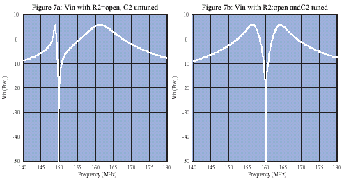
Unshort R2 (R3=R4=0) and examine Vin response as shown in Figure 7a. Here we have C1 tuned for 160 Mhz but C2 is still tuned for 150 Mhz. This is quite different from the response in Figure 3. C2 needs to be trimmed such that there is a single deep null centered at 160 Mhz. C2 after trimming is shown in Figure 7b.
STEP 4:
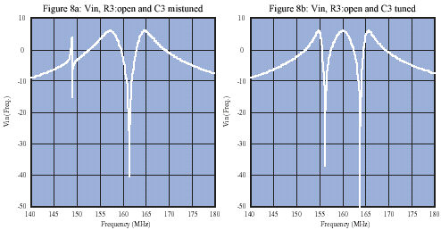
Now unshort R3 (R4=0) and examine Vin response as shown in Figure 8a. C1 and C2 are tuned properly for 160 Mhz but C3 is tuned for 150 Mhz. C3 should be trimmed for a peak centered at 160 Mhz with nulls equally spaced about either side of center frequency. Vin response with C3 properly tuned is shown in Figure 8b.
STEP 5:
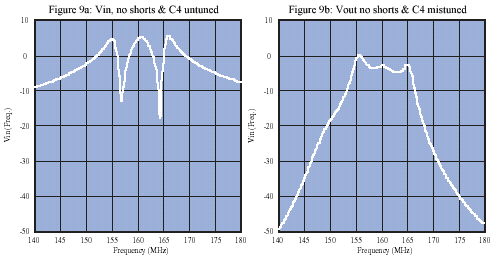
Finally unshort R4 and examine the response of both Vin and Vout as shown in Figures 9a and 9b, respectively. Note that in Figure 9b that a single mistuned capacitor results in a severely deformed filter response. As before C4 is tuned to 150 Mhz instead of 160 Mhz.
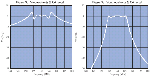
After proper tuning of C4 the Vin and Vout responses appear as in Figures 9c and 9d respectively.
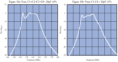
The above examples illustrate several important points. First consider the capacitor component values used in the circuit shown in Figure 1a; C1=C4=23pF and C2=C3=22pF. Note that 22pF is a standard value capacitor while 23 pF is not. Using 22pF for all of the capacitors would result in a response that is not optimal. Although not shown the values for the 160 Mhz filter would be C1=C4=20pF and C2=C3=19.1pF. Once again 19pF is not a standard value. Suppose we used exactly 20pF for all four capacitors; the result would be Figure 10a. Note the 5dB dip in the response. Now suppose we have 5% tolerance 20pF caps (they vary from 21 to 19 pF), so let C1=21, C2=20, C3=20, and C4=19, resulting in the response in Figure 10b.
For most applications the responses in Figure 10 would be unacceptable. Thus trimming would be necessary to guarantee a reasonable filter response.
Practical Considerations:
This tuning procedure could be accomplished quite easily in a production environment if laser trimable resistors were used for R2, R3, and R4 and laser trimable capacitors were used for C1,C2, C3, and C4. R2, R3, and R4 would initially be 0 ohm resistors which could be open circuited by cutting them with a laser. Vin and Vout would be monitored with a network analyzer or spectrum analyzer.
This procedure allows the filter to be tuned in the final product providing that proper attention is given to fixturing such that Vin and Vout can be monitored without loading the circuit.
For more information please contact our Application Engineers.